Pre-plastic lead frame, semiconductor packaging structure and unit thereof, and packaging method

A technology for pre-plasticizing lead wires and lead frames, which is applied in semiconductor devices, semiconductor/solid-state device manufacturing, semiconductor/solid-state device components, etc. Difficulty and production cost, improve quality and yield, reduce the effect of blade loss

Pending Publication Date: 2019-01-22
嘉盛半导体(苏州)有限公司
View PDF2 Cites 3 Cited by
  • Summary
  • Abstract
  • Description
  • Claims
  • Application Information

AI Technical Summary

Problems solved by technology

In this way, when the semiconductor package structure is subsequently cut and separated, the metal connection bar has a relatively high hardness, which causes serious wear on t

Method used


Image

  • Pre-plastic lead frame, semiconductor packaging structure and unit thereof, and packaging method
  • Pre-plastic lead frame, semiconductor packaging structure and unit thereof, and packaging method
  • Pre-plastic lead frame, semiconductor packaging structure and unit thereof, and packaging method

Examples


Example Embodiment

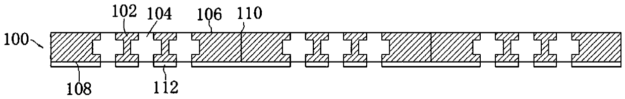
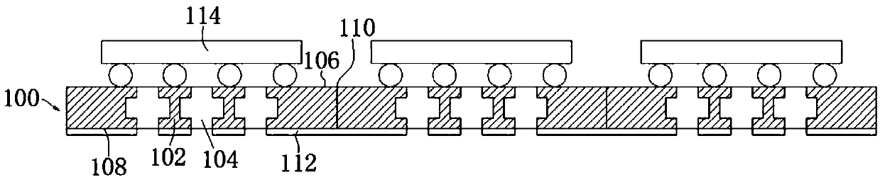
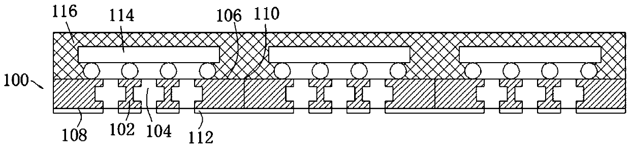
[0062] In order to enable those skilled in the art to better understand the technical solutions in the present invention, the following will clearly and completely describe the technical solutions in the embodiments of the present invention with reference to the accompanying drawings in the embodiments of the present invention. Obviously, the described The embodiments are only a part of the embodiments of the present invention, rather than all the embodiments. Based on the embodiments of the present invention, all other embodiments obtained by those of ordinary skill in the art without creative work shall fall within the protection scope of the present invention.

[0063] It should be noted that when an element is referred to as being "disposed on" another element, it may be directly on the other element or a central element may also exist. When an element is considered to be "connected" to another element, it can be directly connected to the other element or an intermediate elem...


PUM


Abstract

The invention provides a pre-plastic lead frame, a semiconductor packaging structure and unit thereof, and a packaging method. the pre-plastic lead frame comprises a plurality of lead frame units, thelead frame units at least have a conductive element located on the outermost side, an insulating layer is embedded between the conductive elements of the adjacent lead frame units through a pre-plastic packaging process, and the insulating layer covers at least a part of the outer side walls of the conductive element. As that embodiment of the invention can carry out oxidation protection on the conductive element, the preparation process of the pre-plastic lead frame can be simplified and tightly connected, and the manufacturing cost can be reduced; In addition, the problem of metal residue existing in the prior art cutting is eliminated, and the quality and yield of the packaged product are improved.

Description

technical field [0001] The invention relates to the technical field of semiconductor packaging, in particular to a pre-molded lead frame, a semiconductor packaging structure and its unit, and a packaging method. Background technique [0002] The statements in this section only provide background information related to the present disclosure and may not constitute prior art. [0003] Pre-molded lead frame is a new type of substrate for semiconductor packaging. Its design is flexible and diverse, and it is compatible with various packaging styles, such as flip chip (Flip Chip, FC), wire bonding (Wire Bonding), three-dimensional stacked packaging Wait. It is especially suitable for high-density multi-I / O packaging and can meet the packaging needs of different integrated circuit chips. Its typical structure is that several conductive columns and circuit layers are arranged independently of each other in the molding material. According to the needs of the product, the conductiv...

Claims


Application Information

Patent Timeline
IPC IPC(8): H01L23/495H01L21/48H01L21/67
CPCH01L2224/16245H01L2224/97H01L2924/181H01L2924/00012H01L23/49586H01L21/4821H01L21/67144H01L23/49575
Inventor 余训松朱健荣彭彧郑友君
Owner 嘉盛半导体(苏州)有限公司
Why Eureka
Try Eureka