Embedded silicon substrate fan-out type packaging structure and manufacturing method thereof

A packaging structure, fan-out technology, applied in semiconductor/solid-state device manufacturing, electrical components, electric solid-state devices, etc., can solve problems such as high cost, complex structure and manufacturing process, and achieve low cost, small wiring line width, and improved The effect of heat dissipation

Inactive Publication Date: 2015-11-04
HUATIAN TECH KUNSHAN ELECTRONICS
View PDF7 Cites 32 Cited by
  • Summary
  • Abstract
  • Description
  • Claims
  • Application Information

AI Technical Summary

Problems solved by technology

The structure and process are very complicated and the cost is high

Method used


Image

  • Embedded silicon substrate fan-out type packaging structure and manufacturing method thereof
  • Embedded silicon substrate fan-out type packaging structure and manufacturing method thereof
  • Embedded silicon substrate fan-out type packaging structure and manufacturing method thereof

Examples


Embodiment 1

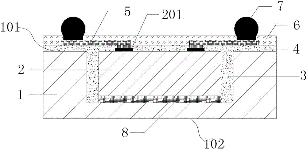
[0045] Such as figure 1 As shown, a fan-out packaging structure embedded in a silicon substrate includes a silicon substrate 1, the silicon substrate has a first surface 101 and a second surface 102 opposite to it, and a direction to the silicon substrate is formed on the first surface. The groove extending from the second surface is preferably a straight groove or an inclined groove with an angle between the side wall and the bottom surface of 80 degrees to 120 degrees, which is not limited here. The schematic diagram of this embodiment is in the shape of a straight groove. A chip 2 is placed in the groove, the pads of the chip face up, and the pads of the chip are close to the first surface; there is adhesion between the chip and the groove bottom of the groove. Layer 8, the chip is bonded to the bottom of the groove through the adhesive layer, which can better fix the chip and prevent the chip from shifting.

[0046] There is a gap between the chip and the sidewall of the...

Embodiment 2

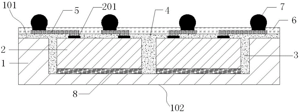
[0069] Such as figure 2 As shown, this embodiment 2 includes all the technical features of embodiment 1, the difference is that two chips 2 are embedded in a groove on the first surface of the silicon substrate, and the size and function of the two chips can be the same or different . This embodiment can expand the functionality of the package.

Embodiment 3

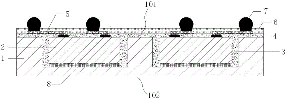
[0071] Such as image 3 As shown, this embodiment 3 includes all the technical features of embodiment 1, and the difference is that two grooves are formed on the first surface of the silicon substrate, and a chip 2 is respectively embedded in each groove, and the two chips The size and function can be the same or different. This embodiment can expand the function of the package body, and at the same time reduce the signal interference between the two chips.

[0072] The invention provides a fan-out packaging structure embedded in a silicon substrate and a manufacturing method thereof. A silicon substrate is used instead of a molding compound as a fan-out substrate, and the advantage of the silicon substrate is fully utilized to produce fine wiring. Utilizing the mature silicon etching process, structures such as holes and grooves can be precisely etched. By embedding the chip in the groove on the silicon substrate, the chip is bonded to the bottom of the groove through the a...


PUM

PropertyMeasurementUnit
thicknessaaaaaaaaaa

Abstract

The invention discloses an embedded silicon substrate fan-out type packaging structure and a manufacturing method thereof. A silicon matrix is adopted to replace molding material to act as a fan-out matrix, and fine wiring can be manufactured by fully utilizing the advantages of the silicon matrix. Holes, grooves and other structures can be accurately etched by utilizing a mature silicon etching technology. Chips are embedded in the grooves on the silicon matrix, the gaps between the chips and the side walls of the grooves are filled by polymer glue and partial welded balls are welded at the surface of the silicon matrix in a fan-out way so that packaging reliability can be enhanced, the technology is simple and cost is low. The silicon matrix has great heat radiation and lower warping so that enhancement of packaging heat radiation is facilitated, adverse warping can be overcome and smaller wiring line width can be acquired, and thus the structure is suitable for high-density packaging. `Wafer plastic packaging and the de-bonding technology can be eliminated as for the aspect of technology so that technology difficulty can be reduced, and thus cost can be substantially reduced and yield rate can be enhanced.

Description

technical field [0001] The invention relates to the technical field of semiconductor packaging, in particular to a fan-out packaging structure embedded in a silicon substrate and a manufacturing method thereof. Background technique [0002] As chips become smaller and the number of I / Os increases, chip-scale packaging can no longer meet the requirements of I / O fan-out. Fan-out wafer-level packaging technology (FOWLP) is a supplement to wafer-level chip size packaging technology. The chip I / O port is led out by reconfiguring the wafer, and solder balls or solder balls are formed on the reconfigured package. Bump terminal array, within a certain range, can replace the traditional wire bonding ball array (WBBGA) package or flip chip ball array (FCBGA) package (<500I / Os) package structure, especially suitable for the booming portable consumer electronics field. [0003] The FOWLP process has been applied since 2008, mainly the eWLB (Embedded Wafer Level BGA) technology of I...

Claims


Application Information

Patent Timeline
Patent Type & Authority Applications(China)
IPC IPC(8): H01L23/488H01L23/06H01L23/18H01L23/373H01L21/50H01L21/56
CPCH01L24/20H01L2224/04105H01L2224/12105H01L2224/73267H01L2224/92244H01L2924/15153H01L2924/157H01L2924/3511H01L2224/32225H01L2924/15156H01L2924/37001H01L2224/2919H01L2224/83191H01L2224/97H01L2924/15155H01L23/3128H01L24/19H01L2224/83H01L21/56H01L23/06H01L23/18H01L23/373H01L23/488
Inventor 于大全
Owner HUATIAN TECH KUNSHAN ELECTRONICS
Why Eureka
Try Eureka