

Multi-ring-arranged double-integrated circuit (IC) chip packaging piece and production method thereof
A technology of chip package and production method, which is applied in the field of multi-circle arrangement carrierless dual-IC chip package, can solve the problems of unsatisfactory ultra-thin packaging products, high density, multi-I/O packaging, etc., and achieve improvement Test yield and reliability, reduce impact, and improve heat dissipation
- Summary
- Abstract
- Description
- Claims
- Application Information
AI Technical Summary
Problems solved by technology
Method used
Image

Examples
Embodiment 1
[0061] Using 8-inch to 12-inch thinning machine, adopts rough grinding, fine grinding and polishing anti-warping process, the wafer with bump chip is thinned to 250μm, rough grinding speed: 6μm / s, fine grinding speed: 1.0μm / s; the thickness of the wafer without bumps is 100μm, the rough grinding speed is 2μm / s, the fine grinding speed is 0.8μm / s, and the chip warpage prevention process is adopted.
[0062] (2), scribing
[0063] Wafers ≤8 inches use DISC 3350 double-knife dicing machine, and wafers from 8 inches to 12 inches use A-WD-300TXB dicing machine, and the scribing speed is controlled at ≤10mm / s.
[0064] (3), one-time loading
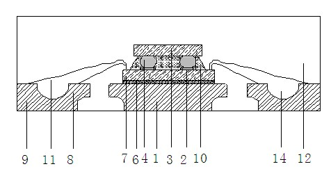
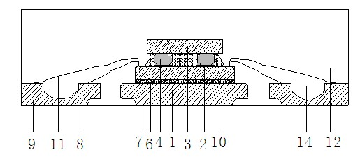
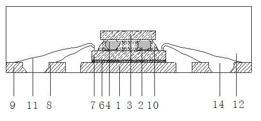
[0065] IC chips 7 with a carrier frame and no bumps are used for one-time chipping, and conductive adhesive 5 is used for one-time chipping. The equipment and process used for chipping and baking are the same as those of ordinary QFN.
[0066] (4), pressure welding
[0067] Carry out wire bonding for the first ...
Embodiment 2
[0087] (1), wafer thinning
[0088] Using 8-inch to 12-inch thinning machine, using rough grinding, fine grinding and polishing anti-warping process, the wafer with bump chip is thinned to 250μm, rough grinding speed: 3μm / s, fine grinding speed: 0.6μm / s; the thickness of the wafer without bumps is 100 μm, the rough grinding speed is 4 μm / s, the fine grinding speed is 0.4 μm / s, and the chip warpage prevention process is adopted.
[0089] (2), scribing
[0090] Wafers ≤8 inches use DISC 3350 double-knife dicing machine, and wafers from 8 inches to 12 inches use A-WD-300TXB dicing machine, and the scribing speed is controlled at ≤10mm / s.
[0091] (3), one-time loading
[0092] Adopt QFN adhesive film (6) and IC chip (7) without concave and convex points, use a core loading machine with adhesive film (6) bonding process, and use a flip chip loading machine for the secondary core of the double chip. The bumps (4) of the IC chip (3) with bumps are dipped with solder (2) and plac...
Embodiment 3
[0114] (1), wafer thinning
[0115] Using 8-inch to 12-inch thinning machine, adopts rough grinding, fine grinding and polishing anti-warping process, the wafer with bump chip is thinned to 250μm, rough grinding speed: 3μm / s, fine grinding speed: 0.6μm / s; the thickness of the wafer without bumps is 100 μm, the rough grinding speed is 4 μm / s, the fine grinding speed is 0.4 μm / s, and the chip warpage prevention process is adopted.
[0116] (2), scribing
[0117] Wafers ≤8 inches use DISC 3350 double-knife dicing machine, and wafers from 8 inches to 12 inches use A-WD-300TXB dicing machine, and the scribing speed is controlled at ≤10mm / s.
[0118] (3), one-time loading
[0119] IC chips 7 with a carrier frame and no bumps are used for one-time chipping, and conductive adhesive 5 is used for one-time chipping. The equipment and process used for chipping and baking are the same as those of ordinary QFN.
[0120] (4), pressure welding
[0121] With embodiment 1.
[0122] (5), ...
PUM
 Abstract
Description
Claims
Application Information