Processing method of a display panel and a display panel

A technology of a display panel and a processing method, which is applied to electrical components, transistors, electrical solid devices, etc., can solve problems such as reducing the parasitic capacitance of the gate layer, and achieve the effects of reducing drift, avoiding miswriting, and reducing parasitic capacitance.

Inactive Publication Date: 2019-01-25
CHONGQING HKC OPTOELECTRONICS TECH CO LTD +1
View PDF13 Cites 0 Cited by
  • Summary
  • Abstract
  • Description
  • Claims
  • Application Information

AI Technical Summary

Problems solved by technology

[0004] The purpose of the present invention is to provide a processing method of a display panel, aiming at solving the problem of how to reduce the parasitic capacitance on both sides of the gate layer

Method used


Image

  • Processing method of a display panel and a display panel
  • Processing method of a display panel and a display panel
  • Processing method of a display panel and a display panel

Examples


Embodiment Construction

[0034] Embodiments of the present invention are described in detail below, examples of which are shown in the drawings, wherein the same or similar reference numerals designate the same or similar elements or elements having the same or similar functions throughout. The embodiments described below by referring to the figures are exemplary and are intended to explain the present invention and should not be construed as limiting the present invention.

[0035] see figure 1 , a method for manufacturing a display panel and a display panel (not shown) produced by using the method for manufacturing a display panel provided by an embodiment of the present invention.

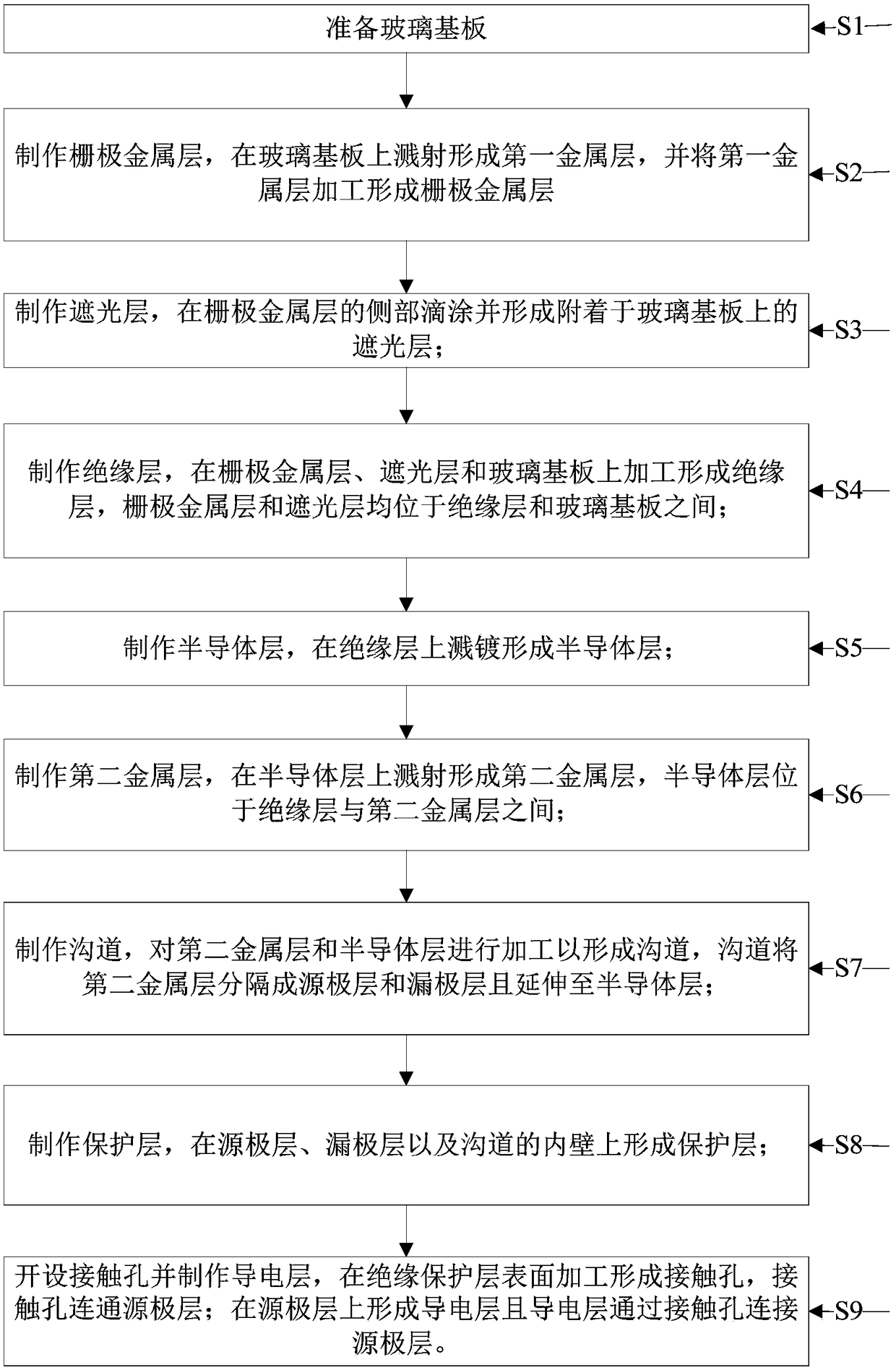
[0036] see figure 1 , Figure 2A-Figure 2F , the processing method of the display panel, comprising the following steps:

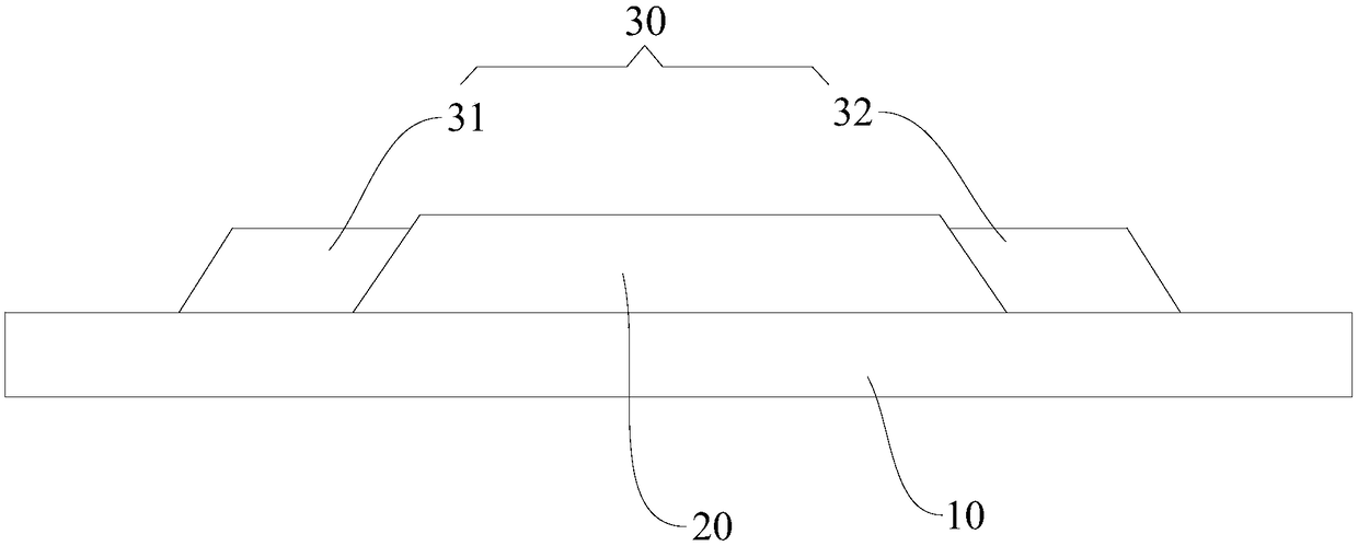
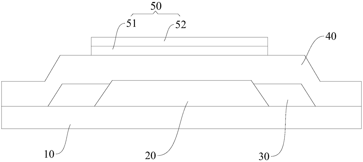
[0037] S1: prepare a cleaned substrate 10, the substrate 10 is generally a glass substrate 10, and the thickness of the glass substrate 10 is generally 0.58-0.52 mm.

[0038] S2: Fabricate the f...


PUM

PropertyMeasurementUnit
thicknessaaaaaaaaaa
thicknessaaaaaaaaaa
thicknessaaaaaaaaaa

Abstract

The invention relates to the technical field of display, in particular to a processing method of a display panel and a display panel. A method for processing the display panel includes preparing a cleaned substrate, sputtering and forming a first metal layer on the substrate, processing the first metal layer to form a gate metal layer, and dropwise coating the side of the gate metal layer to forma light shielding layer attached to the substrate. The light-shielding layer formed by drip coating can effectively reduce the parasitic capacitance of the first metal layer and avoid the miswriting of pixel voltage caused by excessive parasitic capacitance. At the same time, the drift of threshold voltage under bias voltage can be reduced, and the probability of image residue can be reduced.

Description

technical field [0001] The invention relates to the field of display technology, in particular to a processing method of a display panel and the display panel. Background technique [0002] At present, the TFT-LCD (Thin Film Transistor-Liquid Crystal Display) thin film liquid crystal display mainly adopts that each pixel is controlled by a TFT (Thin Film Transistor) switch, the gates of the TFT switches are connected together to form a gate line, and the source layer is connected to the Together they form a signal line. When a voltage is applied to the gate layer G (Gate) of the TFT, the TFT can be turned on, and at the same time, the display data reaches the drain layer D (Drain) of the TFT through the signal line and the turned-on TFT. Form an electric field and charge the liquid crystal to realize the display effect. [0003] The larger the on-state current of the TFT of the ideal TFT-LCD display, the better, and the smaller the off-state current, the better. In order ...

Claims


Application Information

Patent Timeline
Patent Type & Authority Applications(China)
IPC IPC(8): H01L21/84H01L27/12H01L29/786
CPCH01L27/1214H01L27/1259H01L29/78633
Inventor 刘凯军卓恩宗
Owner CHONGQING HKC OPTOELECTRONICS TECH CO LTD
Why Eureka
Try Eureka