Back-illuminated image sensor and manufacture method thereof

A technology of an image sensor and a manufacturing method, which is applied to electric solid-state devices, semiconductor devices, radiation control devices, etc., can solve the problems of high manufacturing cost and complicated manufacturing process, and achieve the effect of simplifying the manufacturing process and reducing the manufacturing cost.

Inactive Publication Date: 2019-01-25
HUAIAN IMAGING DEVICE MFGR CORP
View PDF4 Cites 1 Cited by
  • Summary
  • Abstract
  • Description
  • Claims
  • Application Information

AI Technical Summary

Problems solved by technology

[0006] The invention provides a back-illuminated image sensor and a manufacturing method thereof, which are used to solve the problems of complex manufacturing process and high manufacturing cost of the existing back-illuminated image sensor

Method used


Image

  • Back-illuminated image sensor and manufacture method thereof
  • Back-illuminated image sensor and manufacture method thereof
  • Back-illuminated image sensor and manufacture method thereof

Examples


Embodiment Construction

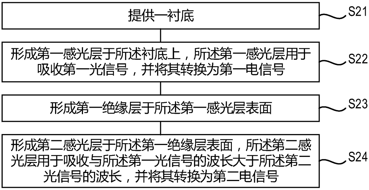
[0047] The specific implementation of the back-illuminated image sensor and the manufacturing method thereof provided by the present invention will be described in detail below in conjunction with the accompanying drawings.

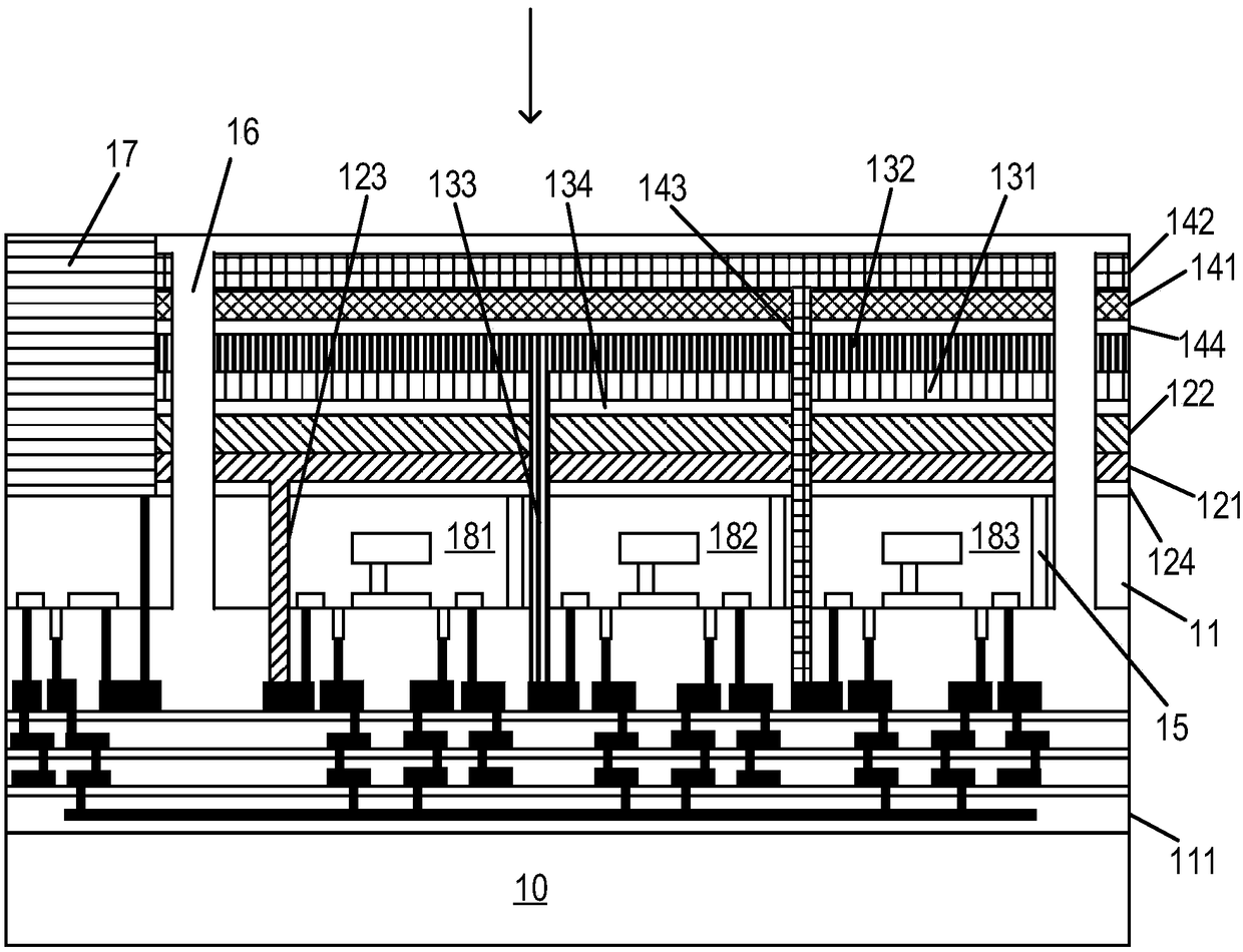
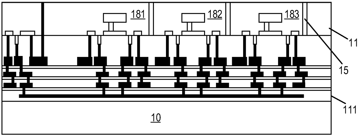
[0048] This specific embodiment provides a back-illuminated image sensor, with figure 1 is a schematic structural diagram of a back-illuminated image sensor in a specific embodiment of the present invention. Such as figure 1 As shown, the back-illuminated image sensor provided in this specific embodiment includes: a substrate with a plurality of pixel regions arranged in a matrix; The first photosensitive layer, the first insulating layer 134, and the second photosensitive layer on the substrate; the first photosensitive layer is used to absorb the first optical signal and convert it into a first electrical signal; the first photosensitive layer An insulating layer 134 is used for electrically isolating the first photosensitive layer and the second phot...


PUM


Abstract

The invention relates to the technical field of semiconductor manufacturing, in particular to a back-illuminated image sensor and a manufacturing method thereof. The backlit image sensor comprises a substrate having a plurality of pixel regions arranged in a matrix; The pixel region has a first photosensitive layer, a first insulating layer and a second photosensitive layer sequentially laminatedon the substrate in a direction perpendicular to the substrate; The first photosensitive layer is configured to absorb a first optical signal and convert it into a first electrical signal; The first insulating layer is used for electrically separating the first photosensitive layer from the second photosensitive layer; The second photosensitive layer is configured to absorb a second optical signalhaving a wavelength different from the first optical signal and convert the second optical signal into a second electrical signal. The invention does not need to provide an optical filter, simplifiesthe manufacturing process of the back-illuminated image sensor, and reduces the manufacturing cost of the back-illuminated image sensor.

Description

technical field [0001] The invention relates to the technical field of semiconductor manufacturing, in particular to a back-illuminated image sensor and a manufacturing method thereof. Background technique [0002] The so-called image sensor refers to a device that converts optical signals into electrical signals. According to different principles, it can be divided into CCD (Charge Coupled Device, Charge Coupled Device) image sensor and CMOS (Complementary Metal-Oxide Semiconductor, metal oxide semiconductor element) image sensor. Since the CMOS image sensor is manufactured using a traditional CMOS circuit process, the image sensor and its required peripheral circuits can be integrated, so that the CMOS image sensor has a wider application prospect. [0003] According to different positions where light is received, CMOS image sensors can be classified into front-illuminated image sensors and back-side illuminated (Back Side Illumination, BSI) image sensors. Among them, co...

Claims


Application Information

Patent Timeline
IPC IPC(8): H01L27/146
CPCH01L27/1461H01L27/1464H01L27/14687
Inventor 吴明吴孝哲林宗贤吴龙江熊建锋薛超
Owner HUAIAN IMAGING DEVICE MFGR CORP
Why Eureka
Try Eureka