Supercharge Your Innovation With Domain-Expert AI Agents!

Cutting device of silicon wafer used for chip manufacturing

A cutting device, silicon wafer technology, applied in the direction of fine working devices, manufacturing tools, working accessories, etc., can solve the problems of inability to meet the cutting requirements of silicon wafer workpieces of different sizes, inability to adjust, poor applicability, etc., to save time , the effect of improving efficiency and improving stability

Inactive Publication Date: 2019-02-01
唐燕
View PDF6 Cites 3 Cited by
  • Summary
  • Abstract
  • Description
  • Claims
  • Application Information

AI Technical Summary

Problems solved by technology

[0003] The technical problem solved by the present invention is to overcome the defects of poor applicability, inability to adjust, and inability to meet the cutting requirements of silicon wafer workpieces of different sizes in the cutting equipment of the prior art, and to provide a cutting device for silicon wafers used in chip manufacturing

Method used


Image

  • Cutting device of silicon wafer used for chip manufacturing
  • Cutting device of silicon wafer used for chip manufacturing

Examples


Embodiment Construction

[0017] The following will clearly and completely describe the technical solutions in the embodiments of the present invention with reference to the accompanying drawings in the embodiments of the present invention. Obviously, the described embodiments are only some, not all, embodiments of the present invention. Based on the embodiments of the present invention, all other embodiments obtained by persons of ordinary skill in the art without making creative efforts belong to the protection scope of the present invention.

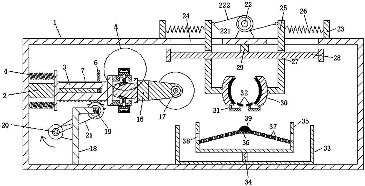
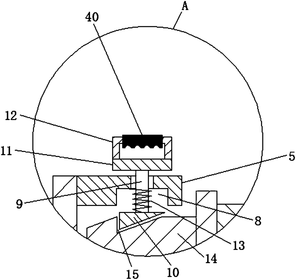
[0018] see Figure 1-2 , the present invention provides a technical solution: a cutting device for silicon wafers used in chip manufacturing, including a housing 1, one side of the inner cavity side wall of the housing 1 is fixedly connected with a guide block 2, and the guide block 2 is covered A sliding sleeve 3 is provided, one side of the sliding sleeve 3 is fixedly connected with a first spring 4, the other end of the first spring 4 is fixedly connected w...


PUM


Abstract

The invention relates to a cutting device of a silicon wafer used for chip manufacturing. The cutting device comprises a shell, a guide block, a slide sleeve, first springs, fixing blocks, a limit block, a limit groove, grooves, movable rods, clamp blocks, movable blocks, handles, second springs, a clamp seat, clamp grooves, a mounting seat, a cutting blade, a wheel stand, a transmission wheel, amotor, a transmission belt, a winding reel, rope rings, a pulling rope, fixing plates, slide grooves, slide blocks, third springs, limit holes, a limit bar, a fixing rod, clamp plates, supports, supporting blocks, a recovery groove, a supporting rod, a chipping collecting groove, a guide plate, chipping collecting holes, discharging grooves, a buffering block and antiskid sleeves. In order to solve technical problems, the cutting device overcomes the defects that cutting equipment in the prior art is poor in applicability and unable to be adjusted, and fails to meet cutting requirements of silicon wafer workpieces of different sizes, and the cutting device has the characteristics that the cutting efficiency and precision are high, the applicability is wide, adjustment is convenient, and cutting requirements of silicon wafers of different sizes can be met.

Description

technical field [0001] The invention relates to the technical field of electronic components, in particular to a silicon wafer cutting device used for chip manufacturing. Background technique [0002] The chip generally refers to the carrier of the integrated circuit, which is also the result of the design, manufacture, packaging, and testing of the integrated circuit. The integrated circuit is the most important part of electronic equipment, which undertakes the functions of computing and storage. The application range of integrated circuits covers Almost all electronic equipment for military and civilian use. Silicon wafers refer to silicon wafers used in the manufacture of silicon semiconductor integrated circuits. Because of their circular shape, they are called silicon wafers. It can be processed into various circuit element structures on the silicon wafer, making it an integrated circuit product with specific electrical functions, so it is the basic raw material for m...

Claims


Application Information

Patent Timeline
Patent Type & Authority Applications(China)
IPC IPC(8): B28D5/02B28D7/00B28D7/02B28D7/04
CPCB28D5/0058B28D5/0076B28D5/0082B28D5/022
Inventor 不公告发明人
Owner 唐燕
Features
  • R&D
  • Intellectual Property
  • Life Sciences
  • Materials
  • Tech Scout
  • Unparalleled Data Quality
  • Higher Quality Content
  • 60% Fewer Hallucinations
Learn More