Array substrate, display panel and display device

An array substrate, the same technology, applied in the display field, can solve the problems of cumbersome production process, many film layers, unfavorable practical application of array substrate, etc., and achieve the effect of simplifying the production process and reducing the film layer

Active Publication Date: 2019-02-01
XIAMEN TIANMA MICRO ELECTRONICS
View PDF7 Cites 28 Cited by
  • Summary
  • Abstract
  • Description
  • Claims
  • Application Information

AI Technical Summary

Problems solved by technology

[0003] However, since the low-temperature polysilicon thin-film transistor and the oxide thin-film transistor in the existing array substrate share less film layers, more metal layers and insulating layers need to be added, which results in more film layers on the array substrate, The production process is more cumbersome
In order to reduce the film layers of the array substrate, it is necessary

Method used


Image

  • Array substrate, display panel and display device
  • Array substrate, display panel and display device
  • Array substrate, display panel and display device

Examples


Embodiment Construction

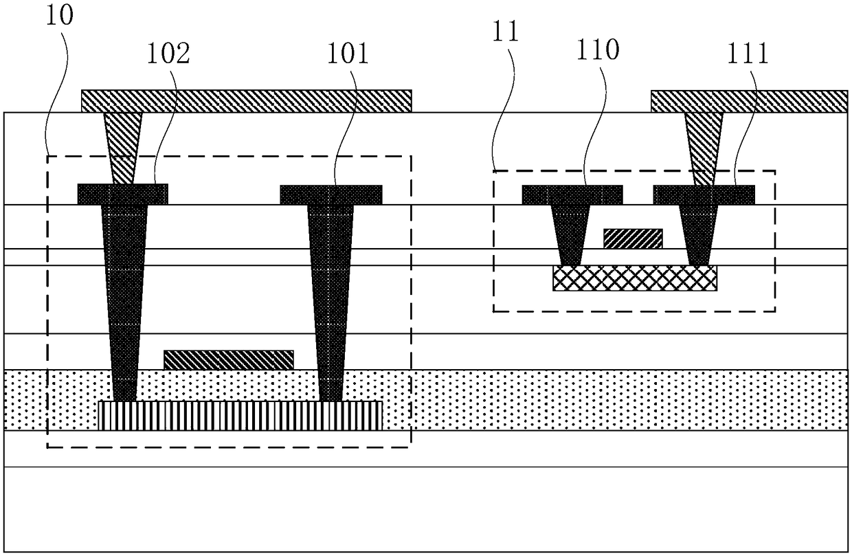
[0037] As mentioned in the background art, the low-temperature polysilicon thin film transistors and the oxide thin film transistors in the existing array substrates share fewer film layers, resulting in more film layers on the array substrate and complicated manufacturing processes. Such as figure 1 as shown, figure 1 It is a schematic cross-sectional structure diagram of an existing array substrate. Even though the source 101 and the drain 102 of the low-temperature polysilicon thin film transistor 10 are arranged on the same layer as the source 110 and the drain 111 of the oxide thin film transistor 11, the array substrate The film layer is still more.

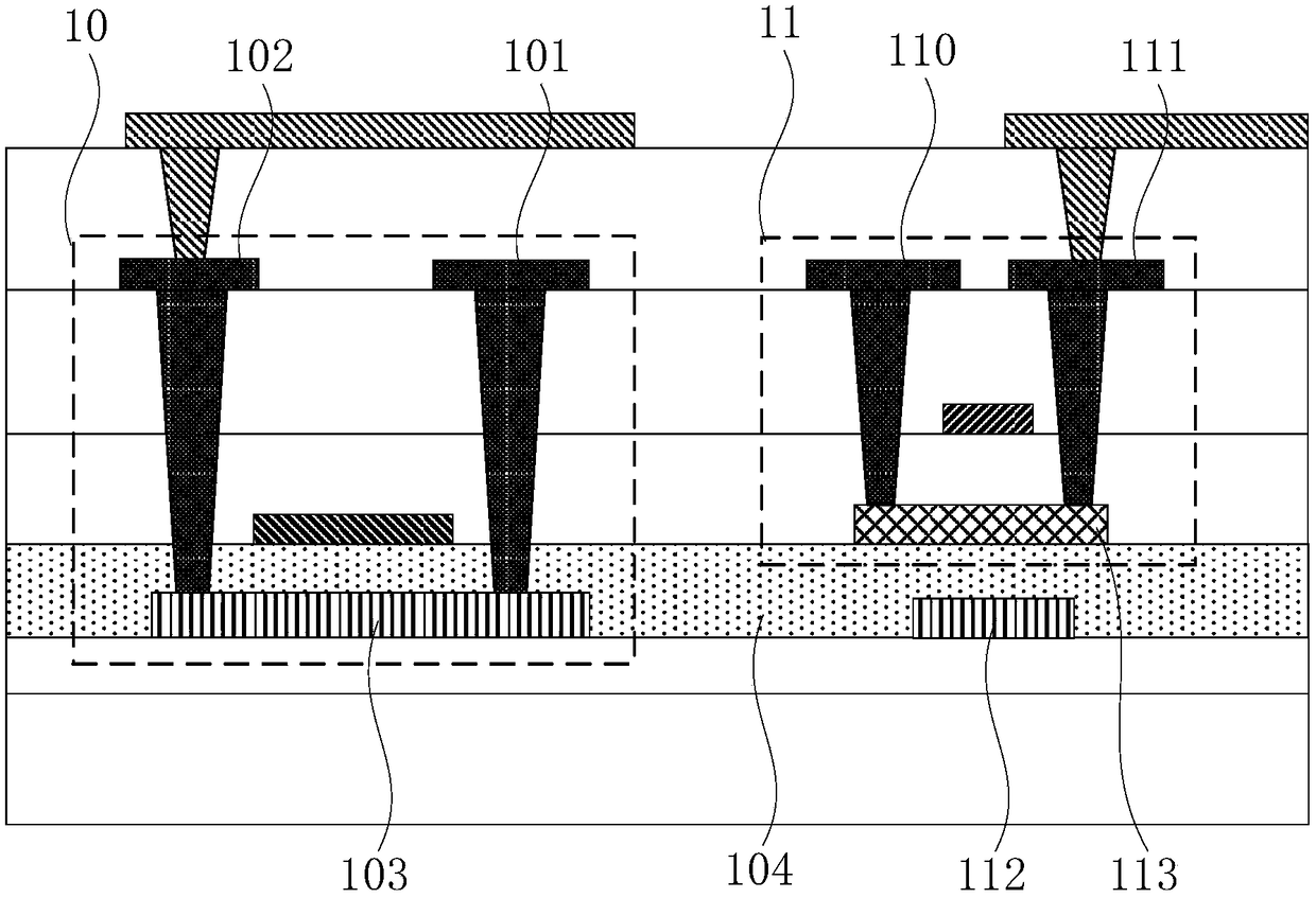
[0038] Such as figure 2 as shown, figure 2 It is a schematic cross-sectional structure diagram of an existing array substrate. In order to minimize the film layer of the array substrate, the inventors set the active layer 103 of the low-temperature polysilicon thin film transistor and the bottom gate 112 of the oxide t...


PUM


Abstract

The invention provides an array substrate, a display panel and a display device. The array substrate comprises a substrate body and first and second thin film transistors (TFT) thereon, and the activelayer material of the first TFT is different from that of the second TFT; the first TFT comprises the first active layer, a first gate, a first source and a first drain, and the first active layer isa low-temperature polycrystalline silicon layer; the second TFT comprises a second active layer, a second gate, a second source and a second drain; the first source, the first drain, the second source and the second drain are positioned in the same layer; and there is a first gate insulating layer between the first active layer and the first gate, and the second active layer is positioned in theslide, close to or far from the substrate, of the first gate insulating layer and does not make direct contact with the first gate insulating layer. Thus, the film layer on the array substrate can bereduced, and the first gate in the first TFT is avoided from influencing influence of the second TFT.

Description

technical field [0001] The present invention relates to the field of display technology, and more specifically, to an array substrate, a display panel and a display device. Background technique [0002] The array substrate is generally divided into a display area and a non-display area surrounding the display area. In the non-display area, low temperature polysilicon-thin film transistor (Low Temperature Poly-silicon-Thin Film Transistor, LTPSTFT) can be used to realize the integration of narrow frame and sensor circuit; in the display area, due to the oxide thin film transistor (OxideThin Film Transistor, Oxide TFT ) has a small leakage current, therefore, the pixel can be driven at a low frequency to reduce power consumption. [0003] However, since the low-temperature polysilicon thin-film transistor and the oxide thin-film transistor in the existing array substrate share less film layers, more metal layers and insulating layers need to be added, which results in more fi...

Claims


Application Information

Patent Timeline
IPC IPC(8): H01L27/12H01L21/77
CPCH01L27/1225H01L27/1229H01L27/127
Inventor 袁永
Owner XIAMEN TIANMA MICRO ELECTRONICS
Why Eureka
Try Eureka