Automatic silicon wafer distributing, conveying and positioning system

A positioning system, silicon wafer technology, applied in conveyors, conveyor objects, conveyor control devices, etc., can solve the problems of low work efficiency, waste of manpower and material resources, etc., to improve the efficiency of slicing, improve the degree of automation and production. Efficiency, saving the effect of self-aligning steps

Pending Publication Date: 2019-02-15
浙江中晶新材料研究有限公司
View PDF1 Cites 6 Cited by
  • Summary
  • Abstract
  • Description
  • Claims
  • Application Information

AI Technical Summary

Problems solved by technology

[0006] Aiming at the deficiencies of the prior art, the present invention provides a self-slicing transfer positioning system for silicon wafers. By setting a loading and lifting mechanism and forming a silicon wafer stacking area on the silicon wafer carrier platform, several silicon wafers are naturally stacked in the silicon wafer stacking area. And move from bottom to top to the bottom of the slicing mechanism. The slicing mechanism contacts the silicon wafers to realize the automatic slicing of the silicon wafers. At the same time, the transmission mechanism continuously transfers them to the self-centering place one by one. Centering, to prepare for the subsequent production of silicon wafers to realize the orderly processing of multiple equipment, save the self-aligning steps before subsequent chamfering processing, improve the automation and production efficiency of silicon wafer processing, and solve the problems in the existing technology. Using the way of manual film placement, the work efficiency is low, and the waste of manpower and material resources is a big technical problem.

Method used


Image

  • Automatic silicon wafer distributing, conveying and positioning system
  • Automatic silicon wafer distributing, conveying and positioning system
  • Automatic silicon wafer distributing, conveying and positioning system

Examples


Embodiment 1

[0063] Embodiments of the present invention are described in detail below, examples of which are shown in the drawings, wherein the same or similar reference numerals designate the same or similar elements or elements having the same or similar functions throughout. The embodiments described below by referring to the figures are exemplary and are intended to explain the present invention and should not be construed as limiting the present invention.

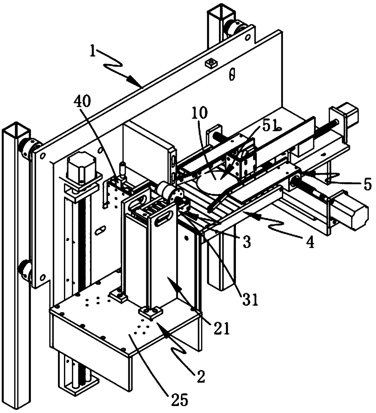
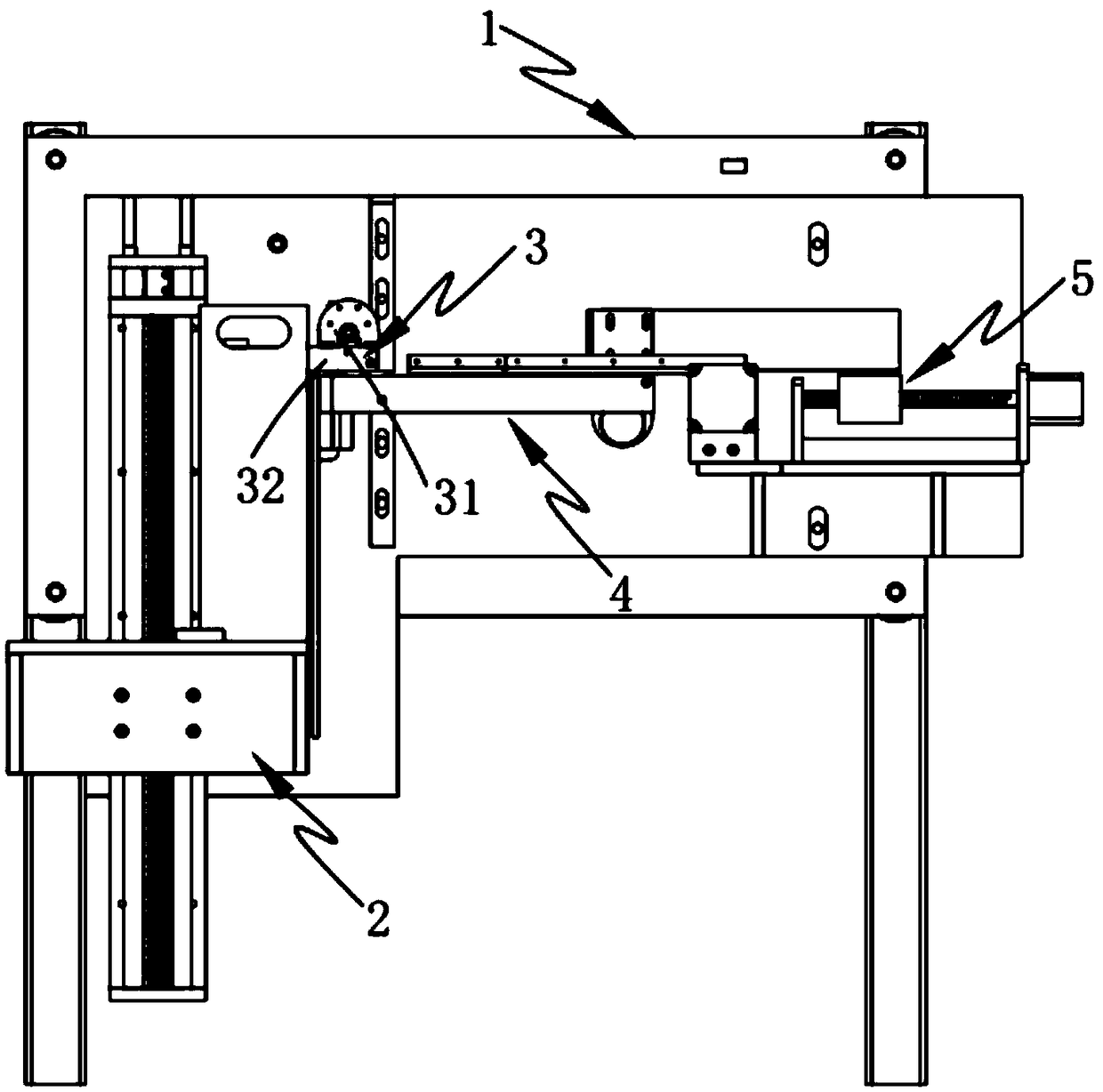
[0064] Such as Figure 1-17 As shown, a silicon chip self-fragmentation transmission and positioning system includes a mounting frame 1, and also includes:

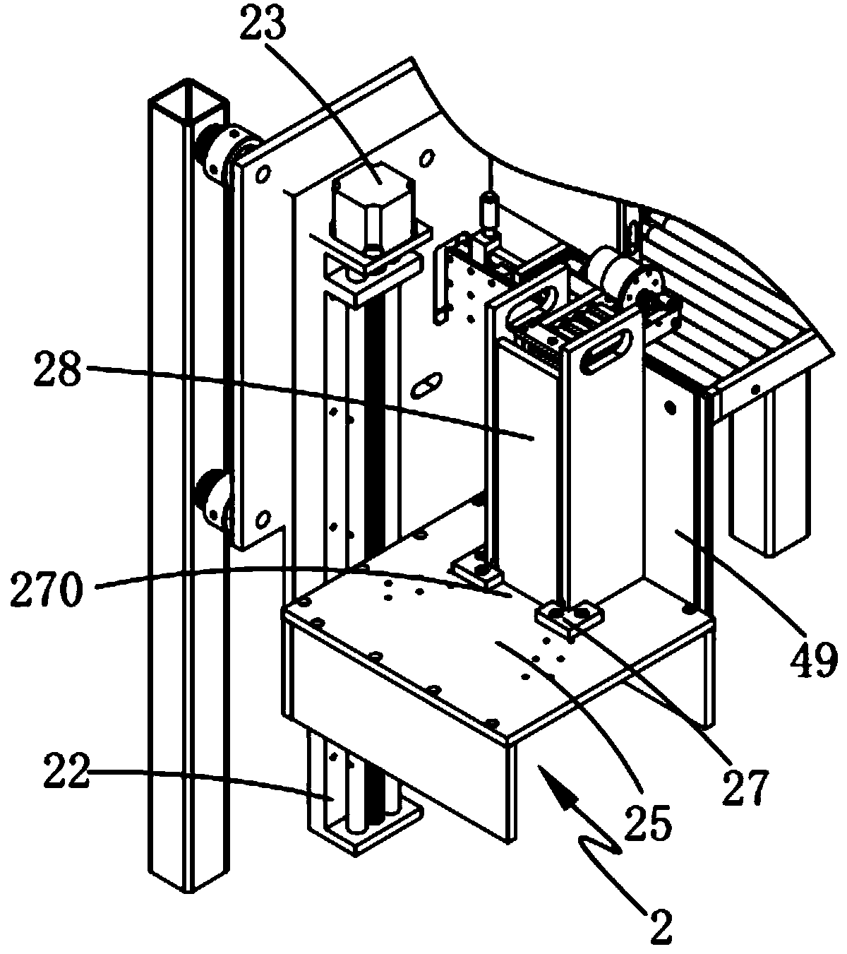
[0065] A feeding lifting mechanism 2, the feeding lifting mechanism 2 is arranged on the installation frame 1, and the feeding lifting mechanism 2 is used to drive the cassette 28 with a plurality of silicon wafers 10 stacked inside to move upward;

[0066] Slicing mechanism 3, said slicing mechanism 3 is arranged on the rear side of said feeding lifting mechanism 2;

[00...


PUM


Abstract

The invention provides an automatic silicon wafer distributing, conveying and positioning system. The system comprises a mounting rack, a feeding and lifting mechanism, a silicon wafer distributing mechanism, a conveying mechanism and a self-centering mechanism, wherein the feeding and lifting mechanism is arranged on the mounting rack and is used for driving a silicon wafer box to upwards move, and a plurality of silicon wafers are overlapped in the silicon wafer box; the silicon wafer distributing mechanism is arranged at the rear side of the feeding and lifting mechanism, and the conveyingmechanism is arranged at the back of the silicon wafer distributing mechanism; and the self-centering mechanism is arranged at the upper part of one end of the conveying mechanism. According to the system, the feeding and lifting mechanism is arranged, and a silicon wafer overlapping area is formed on a silicon wafer bearing platform; a plurality of silicon wafers can be naturally overlapped in the silicon wafer overlapping area and move to the lower part of the silicon wafer distributing mechanism from bottom to top; the silicon wafer distributing mechanism is capable of automatically distributing the silicon wafers while being in contact with the silicon wafers; and meanwhile, the silicon wafers are continuously conveyed to a self-centering part for self-centering in an one-by-one mannerthrough the conveying mechanism; and the technical problems that a mode for manually positioning the silicon wafers is carried out in the prior art, the working efficiency is low, and both labor andmaterials are wasted, can be solved.

Description

technical field [0001] The invention relates to the technical field of monocrystalline silicon wafer production, in particular to a silicon wafer self-slicing transmission and positioning system. Background technique [0002] As a good conductive material, monocrystalline silicon wafers can be widely used in technical fields such as semiconductors and solar cells. In the later stages of the processing of single crystal silicon wafers, steps such as chamfering, grinding, corrosion, polishing and cleaning are generally required. Among them, chamfering refers to trimming the sharp edges of the cut wafers into circular arcs to prevent wafer edge cracking and lattice defects. , so it is a very important process step. [0003] However, the chamfering machine for monocrystalline silicon wafers in the prior art is more complicated to operate, generally only one workpiece can be processed at a time, the workpiece needs to be clamped frequently, and the processing efficiency is very ...

Claims


Application Information

Patent Timeline
Patent Type & Authority Applications(China)
IPC IPC(8): B65G59/06B65G43/08
CPCB65G59/061B65G43/08B65G2201/022
Inventor 万喜增严云黄笑容郑六奎
Owner 浙江中晶新材料研究有限公司
Why Eureka
Try Eureka