Touch display substrate and preparation method thereof, and touch display device

A technology of a touch display substrate and a touch display device, which is applied in the direction of instruments, semiconductor devices, computing, etc., and can solve problems such as unsatisfactory performance of the touch display device, large thickness of the touch display device, and difficult bending of the display device. Achieve the effects of improving production efficiency, avoiding easy breakage, and reducing thickness

Active Publication Date: 2019-02-15
BOE TECH GRP CO LTD +1
View PDF10 Cites 15 Cited by
  • Summary
  • Abstract
  • Description
  • Claims
  • Application Information

AI Technical Summary

Problems solved by technology

Although the effect of color and human-computer interaction is achieved, when the three are superimposed, since the first insulating layer 40 needs to be arranged between the touch layer 20 and the color filter 30, and the first touch electrode 201 of the touch layer 20 The intersection with the second touch electrode 202 needs to be provided with a second insulating layer 50, and the thickness of the first insulating layer 40 and the second insulating layer 50 is about 6000 angstroms. Therefore, setting two insulating layers makes the touch display device thicker. Big
However, the larger thickness of the touch display device will lead to unsatisfactory performance of the touch display device. For example, for a flexible touch display device, the display device will not be easy to bend, and the screen will be easily broken.

Method used


Image

  • Touch display substrate and preparation method thereof, and touch display device
  • Touch display substrate and preparation method thereof, and touch display device
  • Touch display substrate and preparation method thereof, and touch display device

Examples


Embodiment Construction

[0041] The following will clearly and completely describe the technical solutions in the embodiments of the present invention with reference to the accompanying drawings in the embodiments of the present invention. Obviously, the described embodiments are only some, not all, embodiments of the present invention. Based on the embodiments of the present invention, all other embodiments obtained by persons of ordinary skill in the art without making creative efforts belong to the protection scope of the present invention.

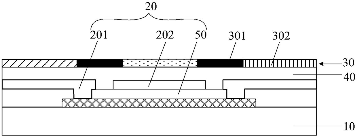
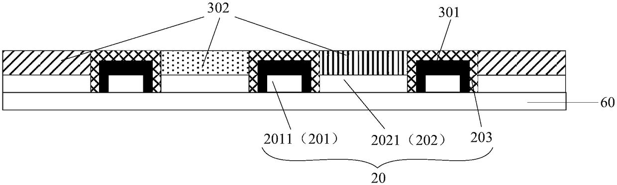
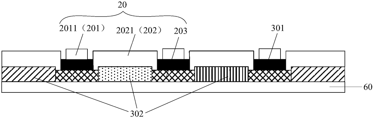
[0042] An embodiment of the present invention provides a touch display substrate, as shown in Figure 2(a), Figure 2(b) and image 3 As shown, it includes: a base substrate 60, a color photoresist pattern 302 arranged on the base substrate 60, and a black matrix pattern (Black Matrix, BM) 301 for spacing the color photoresist pattern 302; also includes: a touch control Layer 20, the touch layer 20 includes a plurality of first touch electrodes 201 arranged in s...


PUM


Abstract

The embodiment of the invention provides a touch display substrate and a preparation method thereof. The touch display device relates to the technical field of touch display and can solve the problemthat the touch display device has a large thickness. A touch display substrate includes a substrate, a color photoresist pattern disposed on the substrate, and a black matrix pattern for spacing the color photoresist pattern. The touch layer includes a plurality of first touch electrodes arranged in order along a first direction and a plurality of second touch electrodes arranged in order along asecond direction. The touch layer includes a plurality of first touch electrodes arranged in order along a first direction and a plurality of second touch electrodes arranged in order along a second direction. Wherein the first touch electrode and the second touch electrode are arranged crosswise, and the crosswise positions are insulated from each other by the black matrix pattern. The inventionis used for reducing the thickness of the touch display device.

Description

technical field [0001] The present invention relates to the technical field of touch display, in particular to a touch display substrate, a preparation method thereof, and a touch display device. Background technique [0002] At present, a touch screen panel (TSP) is an attractive new multimedia human-computer interaction device, which is mainly used in many fields, such as public information inquiry, electronic games, ordering songs and dishes or multimedia teaching, etc. [0003] However, if figure 1 As shown, the existing touch display device ( figure 1 Taking the touch display device as an organic electroluminescent display device (Organic Electro-luminescent Display, referred to as OLED) as an example), the display layer 10, the touch layer 20 and the color filter 30 (Color Filter) are all simple superimposed together. Although the effect of color and human-computer interaction is achieved, when the three are superimposed, since the first insulating layer 40 needs t...

Claims


Application Information

Patent Timeline
Patent Type & Authority Applications(China)
IPC IPC(8): G06F3/041
CPCG06F3/0412G02F1/13338G06F3/0443G06F3/0446G06F2203/04103G06F2203/04111H10K59/40H10K50/865G02F1/1368G06F2203/04102G06F2203/04107
Inventor 漆明春崔艳王钰朱春辉牟山
Owner BOE TECH GRP CO LTD
Why Eureka
Try Eureka