A light-emitting diode epitaxial wafer and its preparation method

A technology of light-emitting diodes and epitaxial wafers, which is applied in semiconductor devices, electrical components, circuits, etc., can solve the problems of reducing the recombination luminous efficiency of electrons and holes, and achieves improving the recombination luminous efficiency, improving crystal quality, and alleviating quantum confinement. The effect of the gram effect

Active Publication Date: 2021-02-19
HC SEMITEK ZHEJIANG CO LTD
View PDF8 Cites 0 Cited by
  • Summary
  • Abstract
  • Description
  • Claims
  • Application Information

AI Technical Summary

Problems solved by technology

[0006] The embodiment of the present invention provides a light-emitting diode epitaxial wafer and a preparation method thereof, which can solve the problem that the lattice mismatch between quantum wells and quantum barriers in the prior art reduces the recombination luminous efficiency of electrons and holes in the quantum wells

Method used


Image

  • A light-emitting diode epitaxial wafer and its preparation method
  • A light-emitting diode epitaxial wafer and its preparation method
  • A light-emitting diode epitaxial wafer and its preparation method

Examples


Embodiment Construction

[0027] In order to make the object, technical solution and advantages of the present invention clearer, the implementation manner of the present invention will be further described in detail below in conjunction with the accompanying drawings.

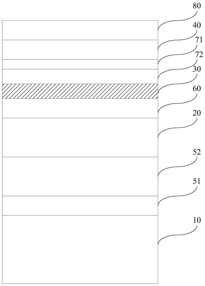
[0028] An embodiment of the present invention provides a light emitting diode epitaxial wafer. figure 1 A schematic structural diagram of a light emitting diode epitaxial wafer provided by an embodiment of the present invention. see figure 1 , the light-emitting diode epitaxial wafer includes a substrate 10, an N-type semiconductor layer 20, an active layer 30, and a P-type semiconductor layer 40, and the N-type semiconductor layer 20, the active layer 30, and the P-type semiconductor layer 40 are sequentially stacked on the substrate 10 superior.

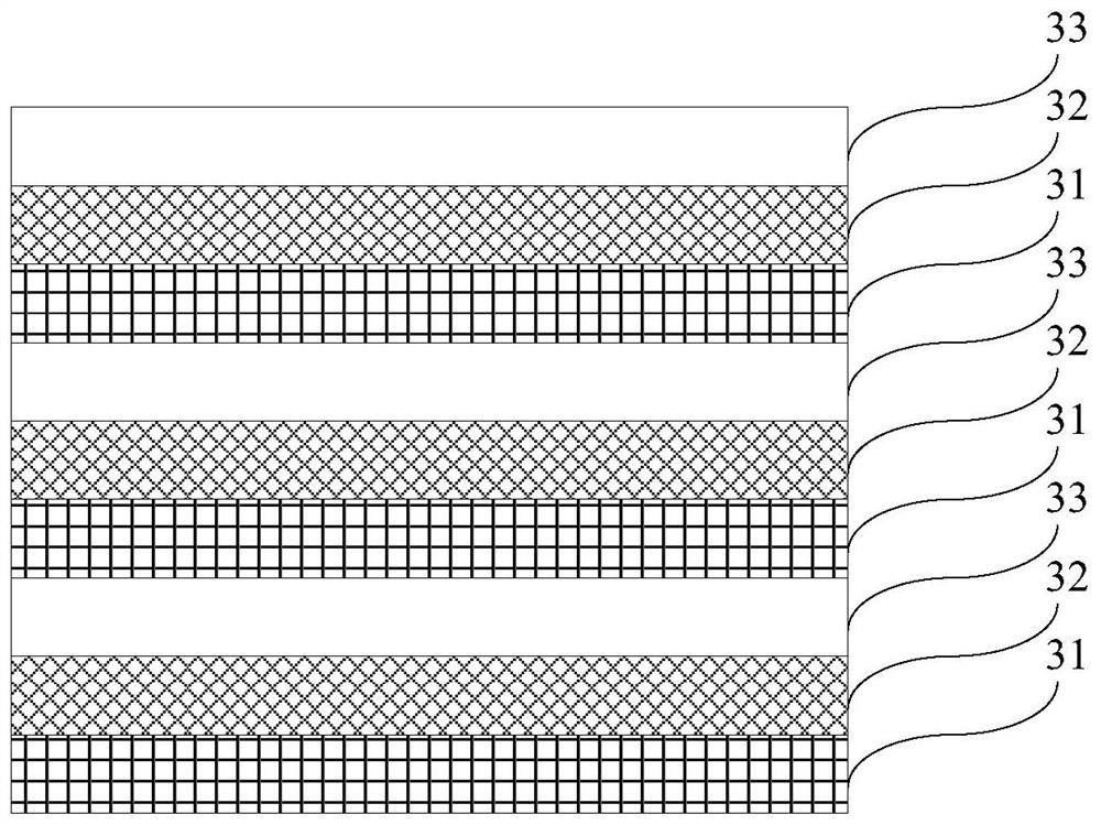
[0029] figure 2 A schematic structural diagram of an active layer provided by an embodiment of the present invention. see figure 2 , in this embodiment, the active layer 30 includes ...


PUM

PropertyMeasurementUnit
thicknessaaaaaaaaaa
thicknessaaaaaaaaaa
thicknessaaaaaaaaaa

Abstract

The invention discloses a light-emitting diode epitaxial wafer and a preparation method thereof, belonging to the technical field of semiconductors. The light-emitting diode epitaxial wafer includes a substrate, an N-type semiconductor layer, an active layer, and a P-type semiconductor layer, and the N-type semiconductor layer, the active layer, and the P-type semiconductor layer are sequentially stacked on the substrate above; the active layer includes a plurality of composite structures stacked in sequence, and each composite structure includes a well layer and a barrier layer stacked in sequence; the material of the well layer is undoped indium gallium nitride, and the The material of the barrier layer is undoped gallium nitride; the composite structure also includes a transition layer, and the transition layer is arranged between the well layer and the barrier layer; the transition layer includes first sublayers stacked in sequence and the second sublayer, the material of the first sublayer is undoped aluminum indium nitride, and the material of the second sublayer is undoped aluminum nitride. The invention can improve the photoelectric performance of the LED.

Description

technical field [0001] The invention relates to the technical field of semiconductors, in particular to a light-emitting diode epitaxial wafer and a preparation method thereof. Background technique [0002] A light-emitting diode (English: Light Emitting Diode, referred to as: LED) is a semiconductor electronic component that can emit light. In the development of the light-emitting diode industry, gallium nitride (GaN), a wide bandgap (Eg>2.3eV) semiconductor material, has developed rapidly and is widely used in lighting, display screens, signal lights, backlights, toys and other fields. [0003] Epitaxial wafers are the primary products in the LED manufacturing process. The existing LED epitaxial wafer includes a substrate, an N-type semiconductor layer, an active layer and a P-type semiconductor layer, and the N-type semiconductor layer, the active layer and the P-type semiconductor layer are sequentially stacked on the substrate. The active layer includes multiple qu...

Claims


Application Information

Patent Timeline
Patent Type & Authority Patents(China)
IPC IPC(8): H01L33/06H01L33/12H01L33/32H01L33/00
CPCH01L33/007H01L33/06H01L33/12H01L33/32
Inventor 乔楠李昱桦胡加辉李鹏
Owner HC SEMITEK ZHEJIANG CO LTD
Why Eureka
Try Eureka