Semiconductor manufacturing device

A technology for manufacturing devices and semiconductors, which is applied in the field of semiconductor manufacturing devices and can solve problems such as complex manufacturing processes

Inactive Publication Date: 2019-02-26
SHANGHAI MICRO ELECTRONICS EQUIP (GRP) CO LTD
View PDF5 Cites 6 Cited by
  • Summary
  • Abstract
  • Description
  • Claims
  • Application Information

AI Technical Summary

Problems solved by technology

[0004] The purpose of the present invention is to provide a semiconductor manufacturing device to solve the problem in the prio

Method used


Image

  • Semiconductor manufacturing device
  • Semiconductor manufacturing device
  • Semiconductor manufacturing device

Examples


Embodiment 1

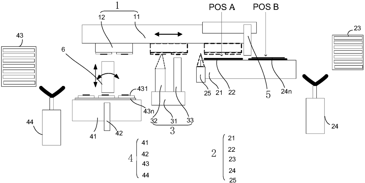
[0023] refer to figure 1 , which is a schematic diagram of the semiconductor manufacturing device provided in Embodiment 1, such as figure 1 As shown, the semiconductor manufacturing device includes: a chip supply module 4, a chip picker 6, a chip transfer module 1, a carrier board supply module 2 and a package module 5, and the chip transfer module 1 includes a transfer module capable of absorbing a plurality of chips 431. stage 12, the carrier board supply module 2 includes a carrier board 22 and a carrier board moving table 21; the chip picker hand 6 picks up a chip from the chip supply module 2 and transfers it to the transfer station 12, and the transfer station 12 carries a plurality of chips and then moves to the bonding station. The carrier board moving table 21 carries the carrier board 22 and then moves to the bonding station. The transfer table 12 is opposite to the carrier board moving table 21 moving, bonding 431n the plurality of chips to the carrier 22 to for...

Embodiment 2

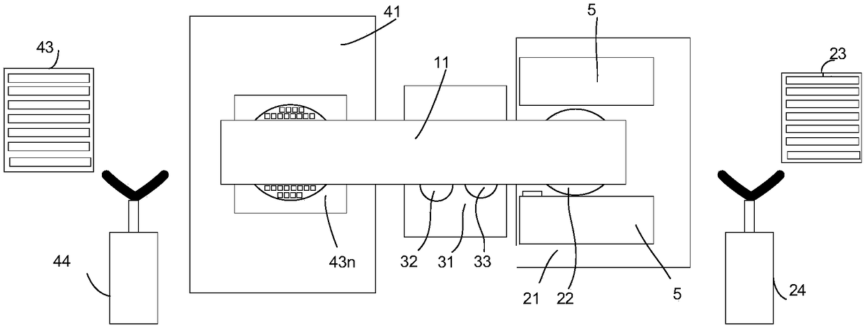
[0031] see Figure 4-Figure 5 , in this embodiment, chip bonding and packaging are not completed in the same step and station, such as Figure 4 As shown, the chip 431 is firstly bonded to the carrier 22 at the POS C station, and then packaged at the POS D station.

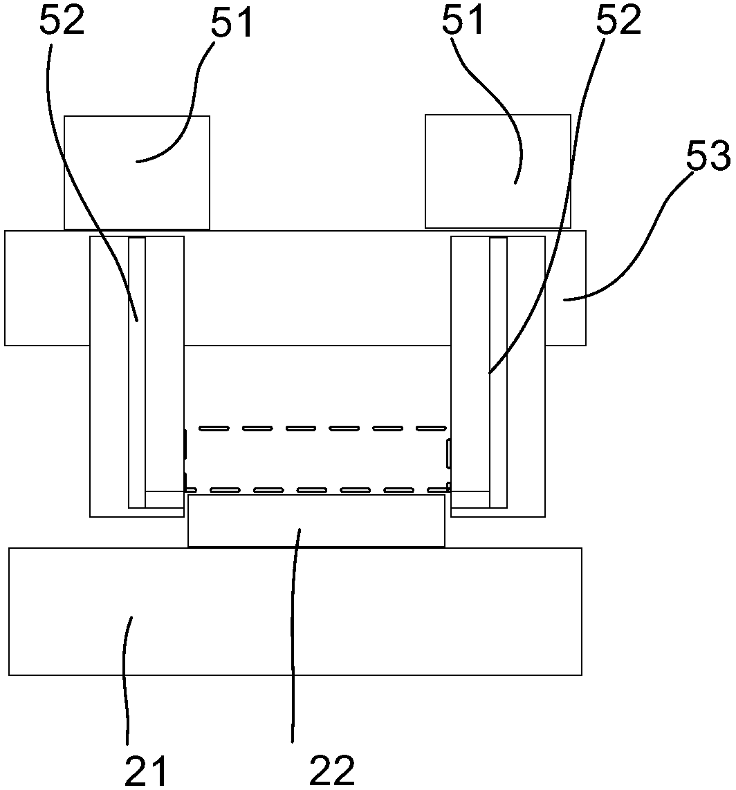
[0032] see Image 6 , in this embodiment, the packaging module 5 not only has a packaging material supply unit 51, an injection molding unit 52 and a packaging motion table 53, but also includes a glue storage supply unit 54 and a glue application unit 55. Preferably, the storage There may be multiple glue supply units 54 and glue application units 55 to increase glue application efficiency. The glue supply unit 54 supplies the bonding glue to the gluing unit 55, and the gluing unit 55 coats the surface of the carrier plate 22 with bonding glue. Preferably, the gluing unit 55 can be used for bonding The glue is pressurized to better control the flow rate of the glue.

[0033] Specifically, the carrier board 22...


PUM


Abstract

The present invention provides a semiconductor manufacturing device. The device comprises a chip supply module, a chip transfer module, a carrier supply module and a package module. The chip transfermodule comprises a chip carrier table capable of absorbing a plurality of chips, the carrier supply module comprises a carrier and a carrier motion table configured to carry a carrier, the chip carrier table is moved to a chip pickup position to hand over the plurality of chips from the chip supply module, the chip transfer module carries the chips to a bonding position, and the chips are bonded onto the carrier to form bonding wafer; and the package module is configured to package the bonding wafer on the carrier motion table to form a package chip. The semiconductor manufacturing device integrates bonding and package to optimize the manufacturing process, reduce the process and reduce the device cost, one device can complete all the work which needs a plurality of devices in the prior art to reduce the device cost. The carrier can be rapidly and repeatedly used to save the current process material cost.

Description

technical field [0001] The invention relates to the field of semiconductor manufacturing, in particular to a semiconductor manufacturing device. Background technique [0002] Chip bonding technology can achieve maximum stacking and integration of chips in a limited area without reducing the line width, and at the same time reduce the chip package volume and line conduction length, thereby improving chip transmission efficiency. Due to the development trend of light, thin and miniaturized electronic products, the application of chip bonding technology is increasing. Combining chip bonding technology with wafer-level packaging technology can produce packages with smaller package size and higher performance. In addition, if the chip bonding process is combined with the TSV (Through Silicon Via) process, a chip structure with more competitive cost and performance can be produced. [0003] Compared with wafer-wafer bonding technology, chip-wafer bonding technology has higher yie...

Claims


Application Information

Patent Timeline
IPC IPC(8): H01L21/67
CPCH01L21/67155H01L21/68H01L21/67742H01L21/67736H01L21/677H01L21/67751H01L21/67754B29C45/14639H01L21/67236H01L21/67721H01L21/6838H01L21/68778H01L21/67132H01L21/67144H01L23/28B29C45/14008B29C65/48B29L2031/34H01L21/67126G11C5/04
Inventor 陈飞彪郭耸
Owner SHANGHAI MICRO ELECTRONICS EQUIP (GRP) CO LTD
Why Eureka
Try Eureka