Electrical devices and electrical equipment

A technology for electrical devices and components, applied in the field of electrical devices and electrical devices, can solve the problems of large commutation loop area, large stray inductance of commutation loop, damage to circuit components, etc. Flow speed, improve coupling effect

Pending Publication Date: 2019-03-05
TSINGHUA UNIV
View PDF0 Cites 3 Cited by
  • Summary
  • Abstract
  • Description
  • Claims
  • Application Information

AI Technical Summary

Problems solved by technology

This arrangement will make the area of ​​the commutation circuit larger, which in turn leads to a larger stray inductance in the commutation circuit
In addition, during or after packaging, the mechanical pressure on the components of the semiconductor device may be much greater than the pressure that the circuit components in the drive module can withstand, which may easily cause damage to the circuit components

Method used


Image

  • Electrical devices and electrical equipment
  • Electrical devices and electrical equipment
  • Electrical devices and electrical equipment

Examples


Embodiment Construction

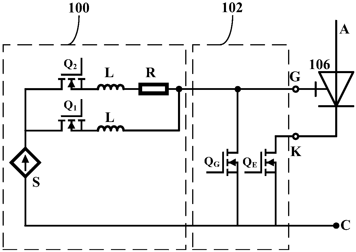
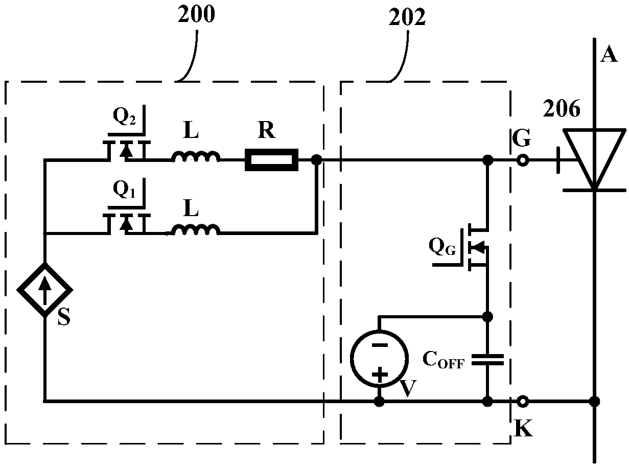
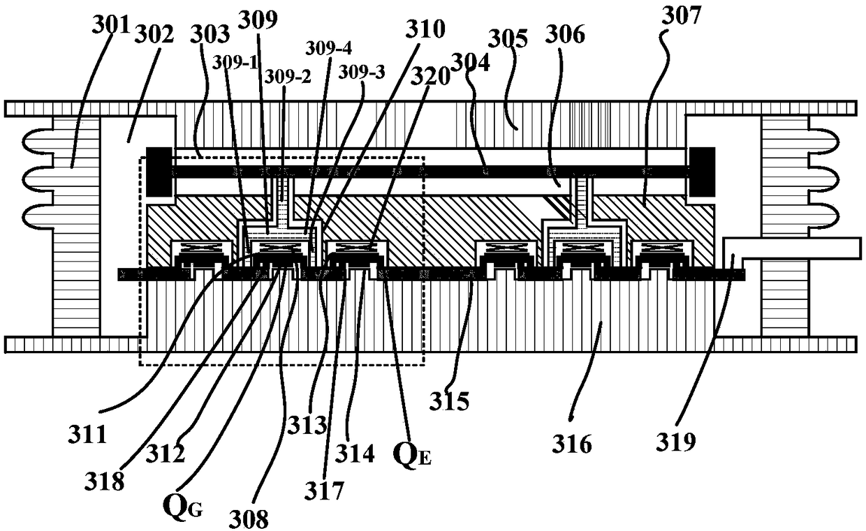
[0035] Various exemplary embodiments of the present disclosure will be described in detail below with reference to the accompanying drawings. However, it should be understood that the descriptions of various embodiments are only illustrative, and are not intended to limit the invention claimed in this application in any way. Unless otherwise specifically stated or the context or its principle is explicit or implied, the relative arrangement, expression and numerical value, etc. of components and steps in the exemplary embodiment are not intended to limit the invention to be protected in the present application.

[0036] The terms used herein are for describing specific embodiments only, and are not intended to limit the present disclosure. As used herein, "a," "a," and "the" in the singular are intended to include the plural forms as well, unless the context clearly dictates otherwise. It should also be understood that when the word "comprising" is used herein, it indicates t...


PUM


Abstract

The invention relates to electrical devices and electrical equipment. An electrical device comprises a semiconductor base plate on which a power semiconductor element is formed, wherein a control electrode and a first current electrode of the power semiconductor element are arranged on a surface of the base plate; a printed circuit board on which a drive module for driving the power semiconductorelement is arranged, wherein the drive module comprises at least one first switching element, and the first switching element comprises a control terminal and current terminals; a first conductive block which is arranged between the base plate and the printed circuit board and provides electrical connection with the first current electrode; one or more connection elements which pass through the first conductive block in a mode of being electrically isolated with the first conductive block and are electrically connected with a part of the control electrode, wherein the connection elements are associated with the corresponding first switching elements; and one or more first spring components which are arranged between the corresponding connection elements and the first switching elements associated with the corresponding connection elements, wherein first current terminals of the first switching elements are electrically connected with a part of the control electrode through utilizationof the connection elements.

Description

technical field [0001] The present disclosure relates to an electrical device including a power element and an electrical device including the same. Background technique [0002] In the face of the rapid development of power electronics technology, users put forward requirements for power semiconductor devices (here also referred to as semiconductor devices or power devices) for fast commutation speed during turn-off period, high turn-off reliability, and good heat dissipation performance. The package structure of a power semiconductor device is particularly critical for a good electrical connection between the semiconductor device and an external circuit, especially for a power semiconductor device suitable for a high-voltage and high-current environment. [0003] With the continuous development of semiconductor technology, higher requirements are put forward for key indicators to measure the performance of power semiconductor devices, such as shutdown current capability or...

Claims


Application Information

Patent Timeline
IPC IPC(8): H01L23/367H01L23/473H01L23/48H01L25/16
CPCH01L25/16H01L23/3677H01L23/473H01L23/481
Inventor 陈政宇曾嵘余占清庄池杰吕纲刘佳鹏
Owner TSINGHUA UNIV
Why Eureka
Try Eureka