LED flip chip and manufacturing method thereof
A technology of flip chip and manufacturing method, which is applied in the direction of electrical components, circuits, semiconductor devices, etc., can solve the problems of high manufacturing cost and cumbersome manufacturing process, and achieve the effects of simple manufacturing process, good light output effect, and cost reduction
- Summary
- Abstract
- Description
- Claims
- Application Information
AI Technical Summary
Problems solved by technology
Method used
Image

Examples
Embodiment Construction
[0057] based on the following Figure 1 to Figure 10 , specifically explain the preferred embodiment of the present invention.
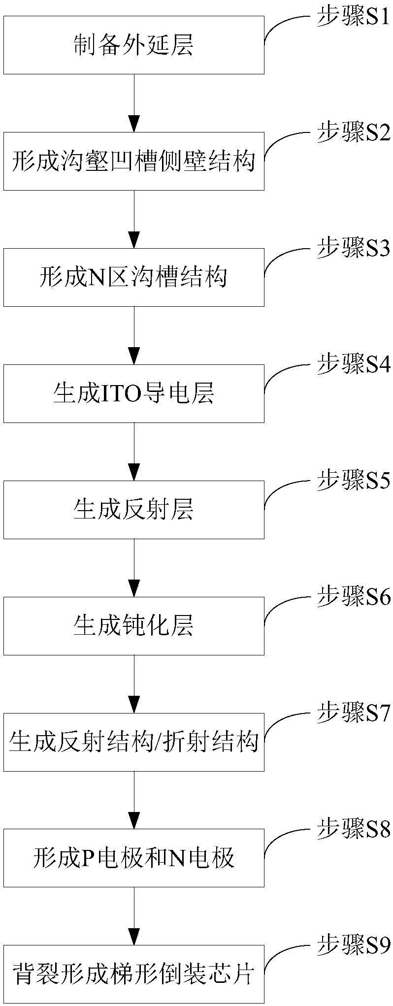
[0058] Such as figure 1 As shown, the present invention provides a LED flip chip manufacturing method, comprising the following steps:
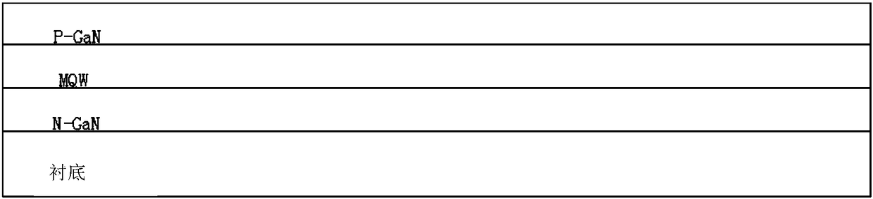
[0059] Step S1, preparing an epitaxial layer;
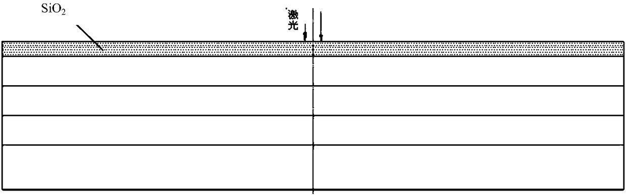
[0060] Step S2, using laser scribing and chemical sidewall etching to form the sidewall structure of the ravine groove;
[0061] Step S3, forming an N-region trench structure by etching between adjacent trench groove sidewall structures, the N-region trench structure is used as the N-region, and the epitaxial layers on both sides of the N-region trench structure are used as the P-region;
[0062] Step S4, generating an ITO conductive layer on the epitaxial layer in the P region;
[0063] Step S5, generating a reflective layer (Ref) on the ITO conductive layer in the P region;
[0064] Step S6, forming a passivation layer on the reflective layer in the P region, an...
PUM
 Abstract
Description
Claims
Application Information