LED (light emitting diode) focus light-emitting device and manufacturing method thereof

A light-emitting device and LED light strip technology, which is applied in the direction of lighting devices, point light sources, lighting device components, etc., can solve the problems of complex lamp structure, troublesome manufacturing, affecting appearance, etc., achieve stable heat dissipation and light efficiency, and save development Cost, the effect of convenient manufacturing and processing

Active Publication Date: 2013-11-13
黎伟强
View PDF3 Cites 0 Cited by
  • Summary
  • Abstract
  • Description
  • Claims
  • Application Information

AI Technical Summary

Problems solved by technology

[0004] Generally, there are two types of existing LED lamps. The first one is to construct an LED lamp tube with single or multiple rows of LEDs. The lampshade is a diffuser or filled with astigmatism materials to ensure that the light is uniform. The disadvantages of this lamp tube are as follows : The lampshade affects the light efficiency of the LED tube. A single LED chip is welded on the PCB, and the whole PCB is then welded or screwed on the aluminum substrate or radiator, which is troublesome to manufacture
The second type is made of chip-on-board panel LED modules, and its cover is transparent and not filled with light-scattering materials. The disadvantage of this lamp structure is that: LED is a panel source, which cannot achieve the light distribution of traditional fluorescent lamps. The packaging board is welded or screwed to the aluminum substrate or heat sink, which is troublesome to manufacture. It is necessary to make the LED aluminum substrate and heat sink closely contact with screws. This kind of lamp has a complicated structure. The LED phosphor is some kind of soft silicone grease, which needs to be covered Protect the LED chip, affect the appearance, and also reduce the light efficiency

Method used


Image

  • LED (light emitting diode) focus light-emitting device and manufacturing method thereof
  • LED (light emitting diode) focus light-emitting device and manufacturing method thereof
  • LED (light emitting diode) focus light-emitting device and manufacturing method thereof

Examples


Embodiment Construction

[0025] The present invention is described in further detail now in conjunction with accompanying drawing. These drawings are all simplified schematic diagrams, which only illustrate the basic structure of the present invention in a schematic manner, so they only show the configurations related to the present invention.

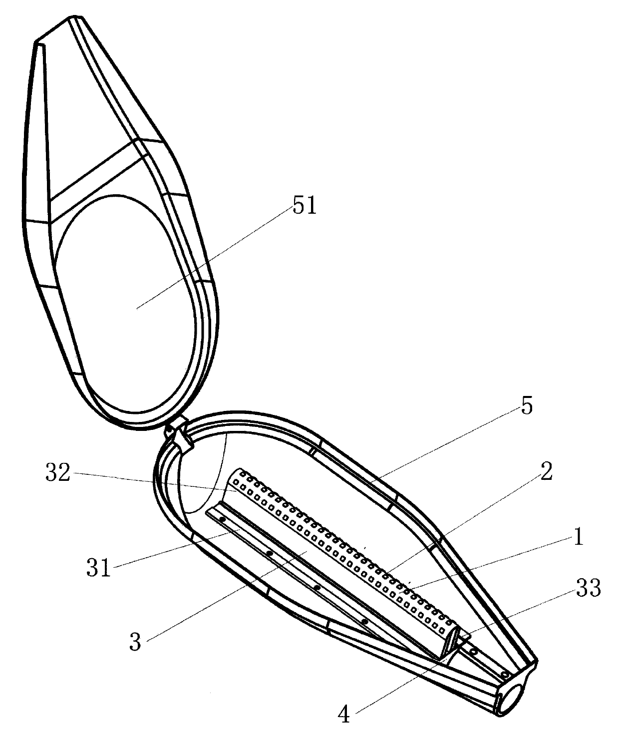
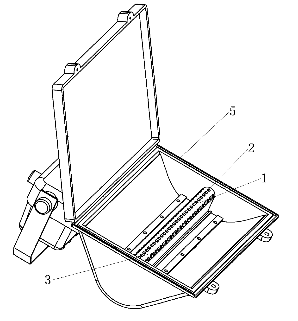
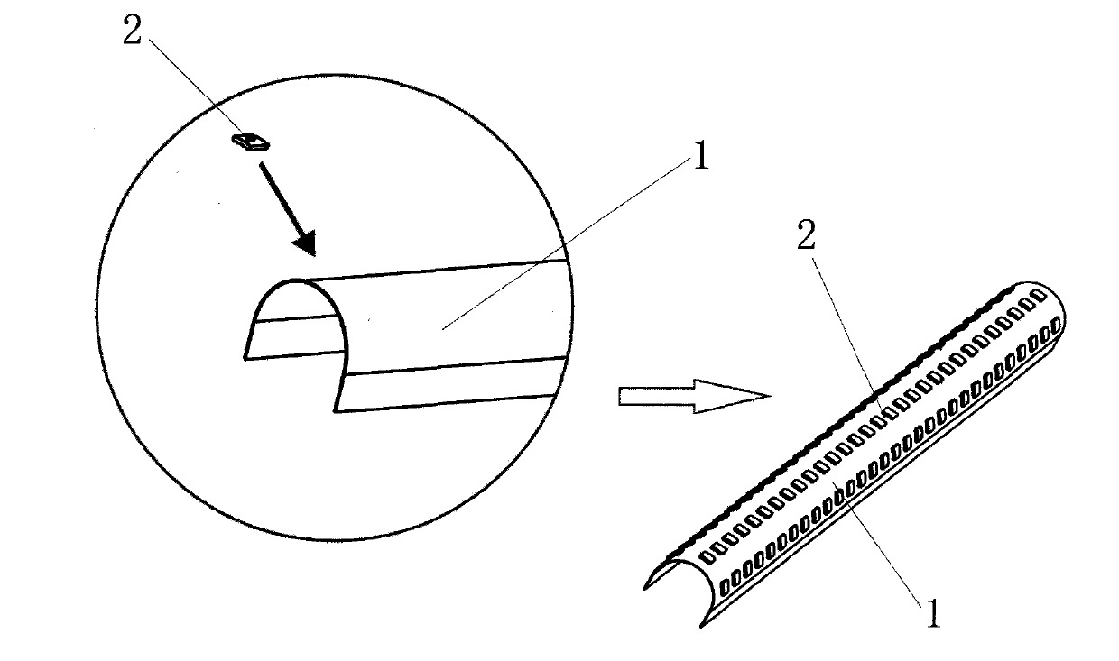
[0026] Such as figure 1 The preferred embodiment of a kind of LED focus light-emitting device of the present invention shown, that is, the specific structural form is the case of a street lamp, which has a copper substrate 1 with a semicircular arc in cross section, a heat-dissipating aluminum substrate 3 and a lampshade 5, along which the copper substrate The side edge of 1 is provided with multiple rows of LED light bars. The LED light bar is composed of several LED lamp beads 2 evenly spaced along the same line. The heat dissipation aluminum substrate 3 has a rectangular base 31, and the rectangular base 31 The top is provided with a raised fin 32 whose to...


PUM


Abstract

The invention relates to an LED (light emitting diode) focus light-emitting device and a manufacturing method thereof. The device is provided with a copper substrate of which the cross section is semicircular, a radiating aluminum substrate and a lampshade, wherein a plurality of rows of LED light bars are arranged along the side edge of the copper substrate; each LED light bar is formed by uniformly distributing a plurality of LED light beads at intervals along the same line; the copper substrate is arranged on the top end of the radiating aluminum substrate and a power access wire of the copper substrate is led out from the side end of the radiating aluminum substrate; and a reflector is arranged below the radiating aluminum substrate. According to the LED focus light-emitting device and the manufacturing method thereof, the LED light beads is pasted on the thin copper substrate, the copper substrate is adhered to the arc-shaped radiating aluminum substrate, a point light source environment is simulated, and the stability of heat dissipation and light effect is guaranteed at the same time, so that point light sources are combined one by one and arranged to form a linear luminous body, and the conversion of luminous point with low power into a luminous surface with high power is realized; and the manufacturing and the processing are convenient, development cost is greatly reduced, enormous social benefit is realized, and the traditional aesthetics of people is satisfied.

Description

technical field [0001] The invention relates to an LED focus lighting device and a manufacturing method thereof. Background technique [0002] In the known technical field, LED (Light Emitting Diode), light-emitting diode, is a solid-state semiconductor device that can convert electrical energy into visible light, and it can directly convert electricity into light. The heart of LED is the wafer of a semiconductor, and one end of wafer is attached on a bracket, and one end is negative pole, and the other end connects the positive pole of power supply, and whole wafer is encapsulated by epoxy resin. Semiconductor wafer is made up of two parts, and a part is P-type semiconductor, and hole occupies an leading position in it, and the other end is N-type semiconductor, and here mainly is electron. But time these two kinds of semiconductors couple together, between them, just form a P-N junction. When electric current acts on this chip by wire time, electron will be pushed to P d...

Claims


Application Information

Patent Timeline
Patent Type & Authority Applications(China)
IPC IPC(8): F21S2/00F21V29/00F21V3/02F21Y101/02F21V29/50F21V29/70
Inventor 黎伟强
Owner 黎伟强
Why Eureka
Try Eureka