Image sensor and forming method thereof

An image sensor and device layer technology, applied in the field of semiconductor technology, can solve problems such as image smearing and charge residue, and achieve good repeatability and reliability

Inactive Publication Date: 2019-03-08
HUAIAN IMAGING DEVICE MFGR CORP
View PDF2 Cites 1 Cited by
  • Summary
  • Abstract
  • Description
  • Claims
  • Application Information

AI Technical Summary

Problems solved by technology

[0004] However, the above-mentioned photodetector with a stacked structure tends to have some residual charge after outputting a frame signal, which causes the problem of image lag.

Method used


Image

  • Image sensor and forming method thereof
  • Image sensor and forming method thereof
  • Image sensor and forming method thereof

Examples


Embodiment Construction

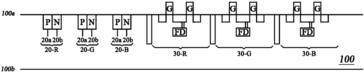
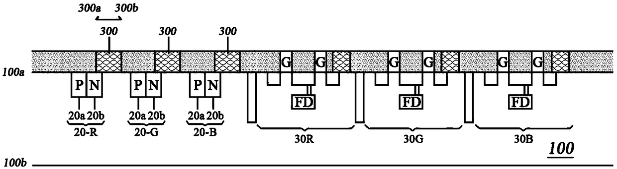
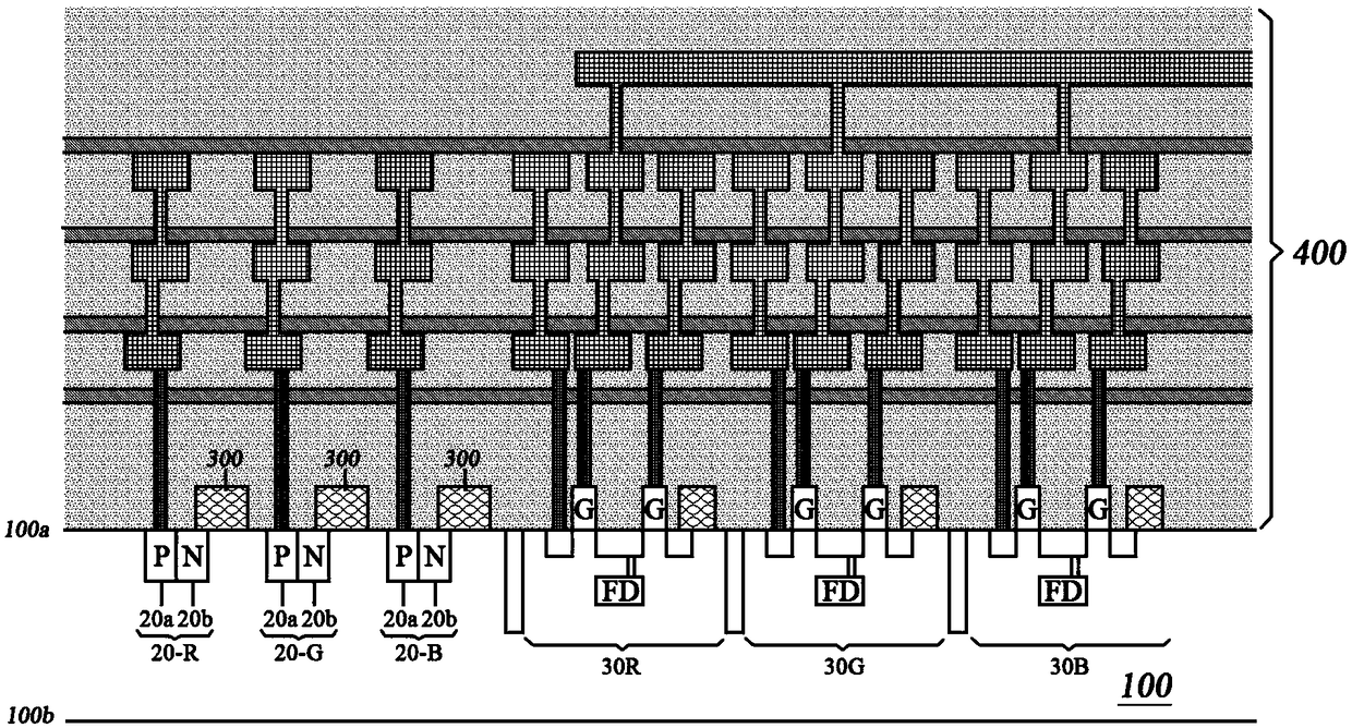
[0018] Below, while referring to the attached Figure 1 Preferred embodiments of the present invention will be briefly described. In addition, the embodiments of the present invention are not limited to the following embodiments, and various embodiments within the scope of the technical idea of ​​the present invention can be employed.

[0019] It will be understood that when an element or layer is referred to as being "on," "adjacent," "connected to" or "coupled to" another element or layer, it can be directly on the other element or layer. A layer may be on, adjacent to, connected to, or coupled to other elements or layers, or intervening elements or layers may be present. In contrast, when an element is referred to as being "directly on," "directly adjacent to," "directly connected to," or "directly coupled to" another element or layer, there are no intervening elements or layers present. Floor. It will be understood that, although the terms first, second, third etc. may ...


PUM


Abstract

The invention provides an image sensor and a forming method thereof. Specifically, the forming method comprises the following steps of providing a device layer substrate, wherein the device layer substrate comprises a first surface and a second surface which are oppositely arranged; forming a diode structure, wherein the diode structure starts at the first surface of the device layer substrate andextends to the second surface of the device layer substrate, and the diode structure comprises a first doping region adjacently arranged in a horizontal direction, and a second doping region with a doping type opposite to that of the first doping region; forming a steering connecting piece which covers the first surface of the device layer substrate, wherein the steering connecting piece has a first side and a second side in the horizontal direction, the first side is electrically connected with the first doping region, and the second side is abutted to the outside of the diode structure; turning over the device layer substrate; forming a connecting plug which extends in a vertical direction and is electrically connected with the second side; and forming a pixel unit comprising three or more photodiodes stacked in the vertical direction, wherein one photodiode is electrically connected with the connecting plug.

Description

technical field [0001] The invention relates to the field of semiconductor technology, and more specifically, the invention relates to an image sensor and a forming method. Background technique [0002] In the image sensor, when light is projected into the photosensitive element, part of the photons will be reflected by the semiconductor material, and the remaining photons will be absorbed by the photosensitive layer in the photosensitive element and excite electron-hole pairs to generate photogenerated carriers, thus completing the photoelectric process. The process of conversion. The wavelengths of different colors of light are different, and the probability of photons being absorbed by the photosensitive layer is different, and the absorption depth is also different: the wavelength of blue light is shorter, the probability of blue light photons being absorbed by the photosensitive layer is higher, and the incident depth is shallower; the wavelength of red light is longer....

Claims


Application Information

Patent Timeline
Patent Type & Authority Applications(China)
IPC IPC(8): H01L27/146
CPCH01L27/1463H01L27/14632H01L27/14636H01L27/14687
Inventor 吴明吴孝哲林宗贤吴龙江熊建锋赵培培
Owner HUAIAN IMAGING DEVICE MFGR CORP
Why Eureka
Try Eureka