
Technology applied to printed circuit board of electric power supply

A printed circuit board, printed circuit technology, applied in the direction of laminated printed circuit boards, printed circuits, printed circuit manufacturing, etc. It can reduce the drilling time, uniform force, and reduce layer migration.

Active Publication Date: 2019-03-08
SICHUAN HAIYING ELECTRONICS TECH
View PDF3 Cites 1 Cited by
  • Summary
  • Abstract
  • Description
  • Claims
  • Application Information

AI Technical Summary

Problems solved by technology

[0006] As the thickness of the copper clad laminate becomes thinner and the number of circuit board layers increases, it is easy to cause interlayer offset and holes during the rivet drilling and riveting process, thereby reducing the yield
[0007] In the subsequent drilling process, the uppermost layer of the circuit board is pressed and drilled with an aluminum plate. This pressing method is conducive to drilling heat dissipation, but it makes the entire circuit board stressed unevenly, and it is easy to cause holes during the drilling process. Offset, as the number of layers of the circuit board increases, the drilling offset becomes more obvious. In severe cases, it even affects the quality of copper sinking, greatly reducing the quality and yield of the circuit board

Method used


Image

  • Technology applied to printed circuit board of electric power supply
  • Technology applied to printed circuit board of electric power supply
  • Technology applied to printed circuit board of electric power supply

Examples


Embodiment Construction

[0038] The technical solution of the present invention will be further described in detail below in conjunction with the accompanying drawings, but the protection scope of the present invention is not limited to the following description.

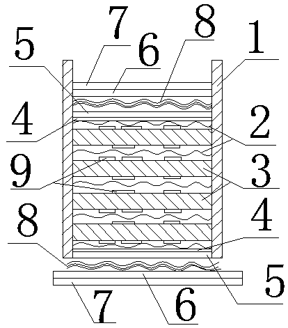
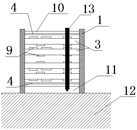
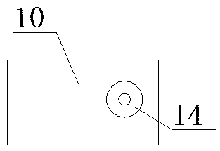
[0039] Such as Figure 1~4 As shown, in this embodiment, the rectangular vertical container 1 is an aluminum rectangular hollow column with openings at both ends, and the length and width of the inner wall of the rectangular hollow column are consistent with the size of the combined circuit board;

[0040] S1. Cutting: cutting out the prepreg 2, the inner layer board 3 and the copper foil 4, so that the length and width of the prepreg 2, the inner layer board 3 and the copper foil 4 are all the same;

[0041] S2. Inner layer graphics: obtain printed circuit graphics on the inner layer board 3 through graphic transfer technology;

[0042] S3. Inner layer etching: the inner layer board 3 with the printed circuit 9 is obtained by etching;

...


PUM


Abstract

The invention discloses a technology applied to the printed circuit board of an electric power supply. The technology comprises the following steps that: S1: carrying out cutting; S2: obtaining an internal-layer graph; S3: carrying out internal-layer etching; S4: carrying out internal-layer AOI (Automated Optical Inspection); S5: carrying out lamination; S6: drilling a hole; S7: carrying out copper deposition; S8: carrying out full-plate electroplating; S9: manufacturing an external-layer circuit; S10: carrying out external-layer AOI; S11: carrying out screen printing and solder resisting; S12: carrying out surface treatment; and S13: forming. In the S5, a traditional rivet riveting process is omitted. In the S6, a magnetic workbench is adopted to lower hole drilling deviation, and therefore, the quality and the rate of finished products of the circuit board of the electric power supply are improved.

Description

technical field [0001] The invention belongs to the field of printed circuit board manufacturing technology, and in particular relates to a technology of electric power printed circuit board. Background technique [0002] The power supply circuit board is an important supporting component of electronic components, and it is also one of the important components of the electronics industry. It is used in almost every kind of electronic equipment, ranging from electronic watches and calculators to computers and communication electronic equipment. , Military weapon systems, etc. [0003] With the development of electronic technology, the thickness of copper clad laminates is getting thinner and thinner, and power supply circuit boards are also developing from single-layer boards to multi-layer boards. At present, they mainly include 6-layer boards, 8-layer boards, 10-layer boards, 14-layer boards, etc. . [0004] The existing production process of power supply circuit board ma...

Claims


Application Information

Patent Timeline
IPC IPC(8): H05K3/00
CPCH05K3/0047H05K3/0058
Inventor 陶应国李旭王青木
Owner SICHUAN HAIYING ELECTRONICS TECH
Learn More