
Hole transport material and quantum dot light emitting diode

A hole-transporting material and quantum dot light-emitting technology, applied in electrical components, circuits, organic chemistry, etc., can solve the problems of low material utilization, high cost, poor product yield, etc., to achieve high interface stability and improve efficiency. and longevity, the effect of 100% solvent resistance

Inactive Publication Date: 2019-03-12
苏州欧谱科显示科技有限公司
View PDF6 Cites 5 Cited by
  • Summary
  • Abstract
  • Description
  • Claims
  • Application Information

AI Technical Summary

Problems solved by technology

[0002] The flat panel display industry is a strategic industry for my country's economic development. As an emerging display industry, organic light-emitting diodes (OLEDs) have entered the stage of mass production. Low, poor product yield, high cost

Method used


Image

  • Hole transport material and quantum dot light emitting diode
  • Hole transport material and quantum dot light emitting diode
  • Hole transport material and quantum dot light emitting diode

Examples


Embodiment 1

[0032] Embodiment 1: the synthesis of compound 1

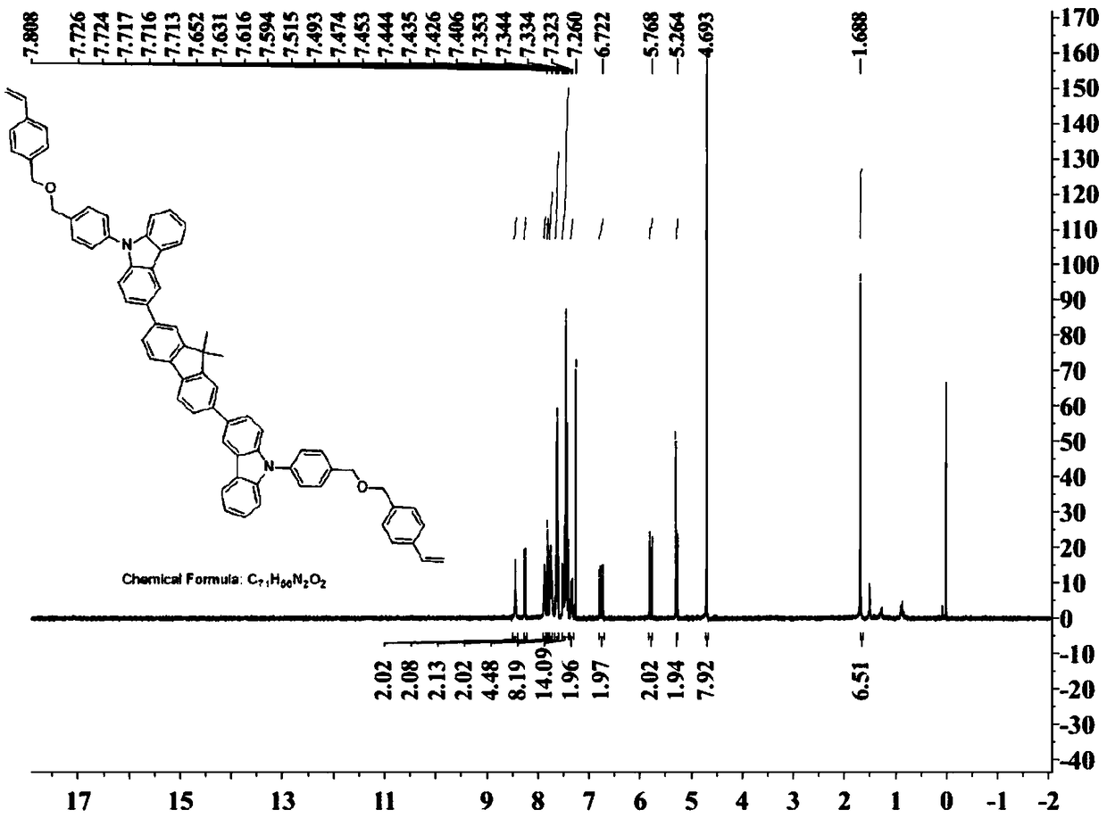
[0033] Material 1 (SM-1) and 3 equivalents of base (NaOH) were dissolved in an appropriate amount of DMF (N,N-dimethylformamide), and replaced with nitrogen three times. Then weigh 3 equivalents of material 2 (SM-2) and dissolve it in an appropriate amount of DMF, add it dropwise to the above solution at room temperature under the protection of nitrogen, and stir the reaction overnight. After the reaction, the reaction solution was poured into water to precipitate a white solid, and the obtained solid was fully washed with water and alkaline solution to obtain the target product 1, the yield: 85%, elemental analysis: C, 87.95%; H, 5.80%; N, 2.87% (measured value); C, 87.98; H, 5.82; N, 2.89 (C 71 h 56 N 2 o 2 Theoretical value), hydrogen spectrum such as figure 1 shown.

[0034] Synthetic route 1:

[0035]

Embodiment 2

[0036] Embodiment 2: the synthesis of compound 2

[0037] Material 3 (SM-3) and 3 equivalents of base (KOH) were dissolved in an appropriate amount of DMF, and replaced with nitrogen three times. Then weigh 3 equivalents of material 2 (SM-2) and dissolve it in an appropriate amount of DMF, add it dropwise to the above solution at room temperature under the protection of nitrogen, and stir the reaction overnight. After the reaction, the reaction solution was poured into water to precipitate a white solid, and the obtained solid was fully washed with water and lye to obtain the target product 2, the yield: 90%, elemental analysis: C, 87.65%; H, 6.87%; N, 2.49% (measured value); C, 87.69; H, 6.90; N, 2.52 (C 81 h 76 N 2 o 2 theoretical value).

[0038] Synthetic route 2:

[0039]

Embodiment 3

[0040] Embodiment 3: the synthesis of compound 3

[0041] Material 4 (SM-4) and 3 equivalents of base (NaH) were dissolved in an appropriate amount of DMF, and replaced with nitrogen three times. Then weigh 3 equivalents of raw material 2 (SM-2) and dissolve it in an appropriate amount of DMF, and add it dropwise to the above solution under the protection of nitrogen at room temperature, and stir the reaction overnight. After the reaction, the reaction solution was poured into water to precipitate a white solid, and the obtained solid was fully washed with water and lye to obtain the target product 3, the yield: 60%, elemental analysis: C, 87.60%; H, 7.25%; N, 2.41% (measured value); C, 87.59; H, 7.26; N, 2.40; (C 85 h 84 N 2 o 2 theoretical value).

[0042] Synthetic route 3:

[0043]


PUM

PropertyMeasurementUnit
surface roughnessaaaaaaaaaa

Abstract

The invention discloses a hole transport material which has high hole transport property and hole injecting property after being crosslinked, thereby improving the efficiency and lifetime of a device.The invention further discloses a quantum dot light emitting diode which is long in life and high in efficiency. The hole transporting material comprises a compound as shown in the general formula I,as shown in the specification, wherein R1 and R2 are independently selected from C1-C30 alkyl.

Description

technical field [0001] The invention relates to the technical field of photoelectric materials, in particular to hole transport materials and quantum dot light-emitting diodes. Background technique [0002] The flat panel display industry is a strategic industry for my country's economic development. As an emerging display industry, organic light-emitting diodes (OLEDs) have entered the stage of mass production. However, the existing commercial OLEDs are mainly prepared by vacuum evaporation, which has a material utilization rate Low, poor product yield, and high cost. The printing display technology is considered to be an inevitable development trend of large-size flat panel displays in the future due to its advantages such as high material utilization rate, simple preparation process, and large-scale large-scale production. Among them, the quantum dot light-emitting diode device (QLED), which uses inorganic quantum dot materials instead of organic light-emitting materials,...

Claims


Application Information

Patent Timeline
Patent Type & Authority Applications(China)
IPC IPC(8): C07D209/86H01L51/50H01L51/54
CPCC07D209/86H10K85/615H10K85/6572H10K50/15
Inventor 苏文明刘扬李宛飞谢黎明纪学珍王邈
Owner 苏州欧谱科显示科技有限公司
Learn More