Chip test method based on FPGA/MCU

A chip testing and chip technology, applied in the field of chip testing based on FPGA/MCU, can solve the problems of long time period, high cost of returning to the factory, difficult to implement, etc., and achieve the effect of good real-time performance and convenient after-sales maintenance.

Inactive Publication Date: 2019-03-29
XIAN INTELLIGENCE SILICON TECH INC
View PDF5 Cites 6 Cited by
  • Summary
  • Abstract
  • Description
  • Claims
  • Application Information

AI Technical Summary

Problems solved by technology

[0004] However, after leaving the mass production environment, it is difficult to perform a full performance test on the chip within the company. The cost of returning to the factory for te

Method used


Image

  • Chip test method based on FPGA/MCU
  • Chip test method based on FPGA/MCU
  • Chip test method based on FPGA/MCU

Examples


Embodiment 2

[0076] The embodiments of the present invention further describe the chip testing method of the present invention by taking a CPLD chip as an example on the basis of the above-mentioned embodiments.

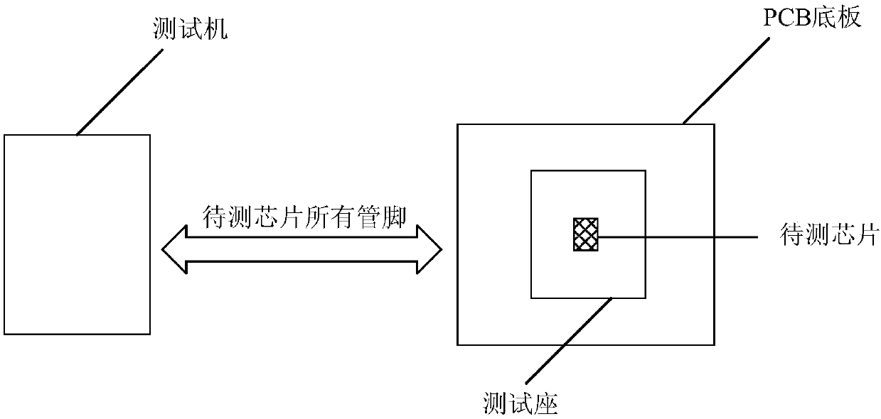
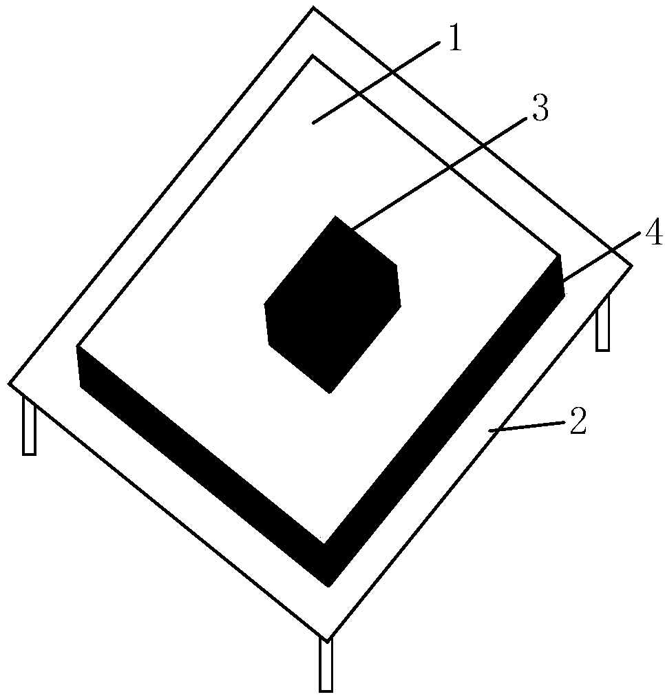
[0077] Step 1: Place the CPLD chip to be tested in the test seat 3 , wherein the test seat 3 is located on the daughter board 1 .

[0078] Step 2: Connect the pins of the CPLD chip to be tested with the I / O pins of the FPGA chip 5 on the test board through pin headers.

[0079] The pins of the CPLD chip to be tested correspond to the I / O pins of the FPGA chip one by one.

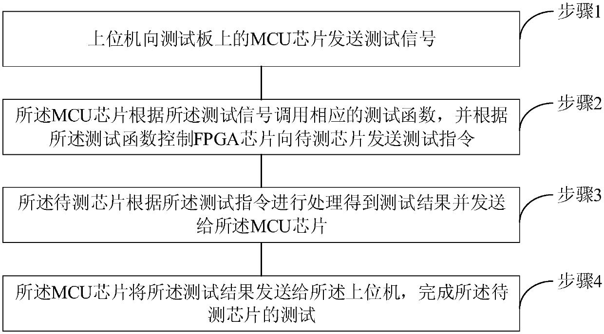
[0080] Step 3: The host computer 7 sends a test signal to the MCU chip 6 on the test board.

[0081] Step 4: The MCU chip 6 calls a corresponding test function according to the test signal, and controls the FPGA chip 5 to send a test command to the CPLD chip to be tested according to the test function.

[0082] Step 5: The CPLD chip to be tested performs processing according to the test instruction to obtain ...


PUM


Abstract

The present invention relates to a chip test method based on an FPGA/MCU. The method comprises the following steps that: a host computer sends a test signal to an MCU chip on a test board; the MCU chip calls a corresponding test function according to the test signal, and controls the FPGA chip to send a test instruction to a to-be-tested chip according to the test function; the to-be-tested chip is processed according to the test instruction to obtain a test result, and the test result is sent to the MCU chip; and the MCU chip sends the test result to the host computer, so that a test on the to-be-tested chip is completed. According to the test method provided by the present invention, the full performance test on the chip in the laboratory can be more facilitated, and the time and economic costs are reduced.

Description

technical field [0001] The invention belongs to the field of integrated circuits, and in particular relates to a chip testing method based on FPGA / MCU. Background technique [0002] Chip, also known as microcircuit (microcircuit), microchip (microchip), integrated circuit (integratedcircuit), refers to a silicon chip containing an integrated circuit, which is small in size and is often part of a computer or other electronic equipment. The carrier of the integrated circuit is also the result of the design, manufacture, packaging and testing of the integrated circuit, usually an independent whole that can be used immediately [0003] See figure 1 , figure 1 A schematic structural diagram of the performance test of a chip provided in the prior art; before the chip reaches the user end, the full performance test of the chip is carried out, and the chips that do not meet the design requirements are screened out. At present, the full performance test of the chip is carried out ...

Claims


Application Information

Patent Timeline
IPC IPC(8): G01R31/28
CPCG01R31/2834G01R31/2886G01R31/2896
Inventor 段媛媛田军贾红程显志陈维新韦嶔
Owner XIAN INTELLIGENCE SILICON TECH INC
Why Eureka
Try Eureka