Photoelectric circuit packaging device based on ceramic carrier board

A circuit packaging and carrier board technology, applied in the field of sensors, can solve the problems of reduced reliability, space redundancy, low thermal conductivity, etc., and achieve the effects of reduced size and height, high-speed circuit design, and high mechanical strength

Inactive Publication Date: 2019-04-05
SHENZHEN FASTPRINT CIRCUIT TECH +1
View PDF6 Cites 0 Cited by
  • Summary
  • Abstract
  • Description
  • Claims
  • Application Information

AI Technical Summary

Problems solved by technology

The disadvantages are: 1. The multi-material construction of the metal and the substrate has redundant space, which invisibly increases the length and width of the package. The organic substrate has a height that cannot be ignored. Installing it on the boss increases the overall metal package. Overall height; 2. The material of the organic substrate belongs to resin glass fiber, which has low thermal conductivity, poor heat dissipation, and low Tg value and low heat resistance; 3. The thermal expansion coefficient difference between the organic substrate and the contacting metal material surface is too large, and The mechanical strength of the substrate is not high and easy to deform, and the substrate is prone to warping, which reduces reliability and can lead to electrical open circuit due to displacement
4. The outer lead frame of the substrate is longer, and the lead inductance is large

Method used


Image

  • Photoelectric circuit packaging device based on ceramic carrier board
  • Photoelectric circuit packaging device based on ceramic carrier board

Examples


Embodiment Construction

[0016] It should be noted that, in the case of no conflict, the embodiments in the present application and the features in the embodiments can be combined with each other.

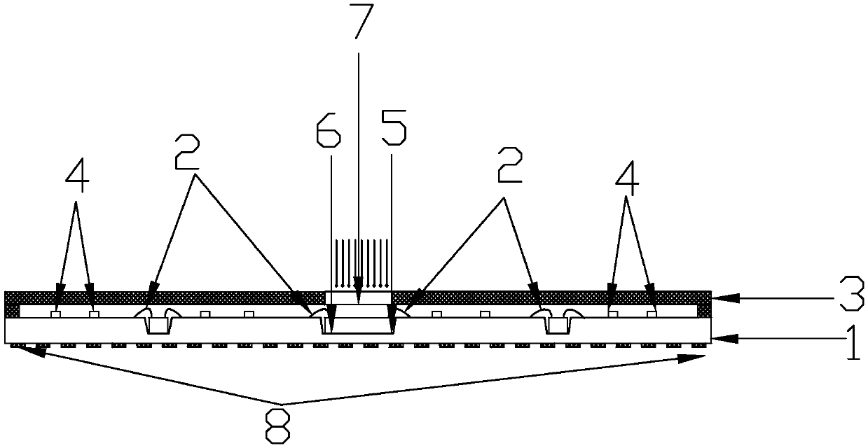
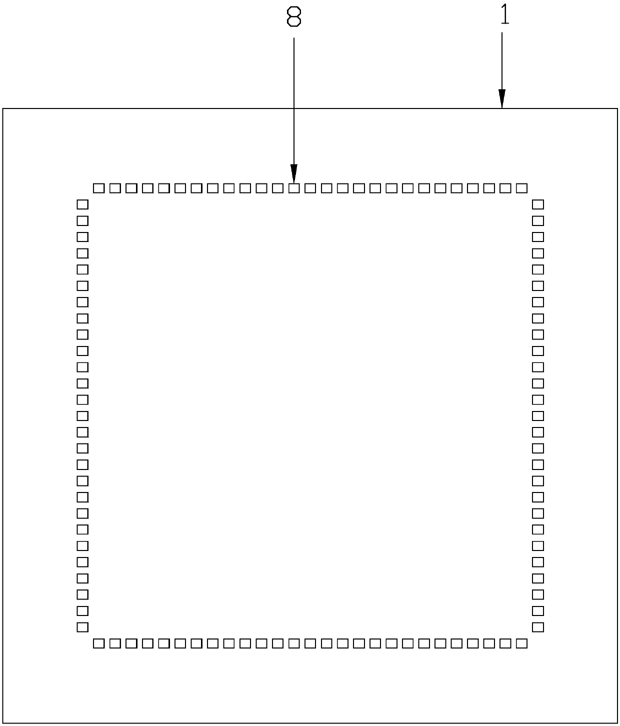
[0017] like figure 1 As shown, it shows a photoelectric circuit packaging device based on a ceramic carrier, which includes a ceramic carrier 1, gold wires 2, and a ceramic cover. The ceramic carrier 1 and the ceramic cover 3 are sealed with a metal Sealed connection (such as brazing method, which is to add some active elements such as Ti and Zr to the solder, and its content is usually below 5%, such as (Ag-28, Cu-12, In-1, Ti) to combine metal and Ceramics are directly brazed), the inner surface of the ceramic carrier plate 1 is provided with circuit lines, the first cavity 5 and the second cavity 4, the first cavity 5 is placed with a photoelectric chip 6, preferably, the first cavity 5 and the depth of the second recess 4 are both 0.5 mm. The photoelectric chip 6 is electrically connected to the peri...


PUM

PropertyMeasurementUnit
Depthaaaaaaaaaa

Abstract

The invention discloses a photoelectric circuit packaging device based on a ceramic carrier board. The photoelectric circuit packaging device comprises a ceramic carrier board, a gold wire and a ceramic cover plate, wherein the ceramic carrier board is in sealed connection with the ceramic cover plate; the inner surface of the ceramic carrier board is provided with a circuit, a first recess and asecond recess; the first recess is provided with a photoelectric chip; a peripheral circuit of the photoelectric chip is disposed in the second recess; and the photoelectric chip is electrically connected to the peripheral circuit through the gold wire. The photoelectric circuit packaging device uses the ceramic carrier board as a substrate and a housing base. The recesses are directly disposed onthe ceramic carrier board and are used for holding the photoelectric chip and its peripheral circuit. The circuit is directly printed on the ceramic carrier board, and an additional metal housing base is not required. Compared with a SIP module package, the size and height are greatly reduced. By means of the advantages of good heat dissipation and high mechanical strength of the ceramic material, the photoelectric circuit packaging device has good heat dissipation and high mechanical strength.

Description

technical field [0001] The invention relates to the technical field of sensors, in particular to a photoelectric circuit packaging device based on a ceramic carrier. Background technique [0002] Now the organic substrate technology is widely used in the packaging industry, especially the vast majority of consumer packaging adopts the organic substrate packaging technology. However, the heat dissipation and airtightness of the organic substrate package are used in a high-temperature and humid environment, and its instability is highlighted. The existing chip optoelectronic module package is processed based on organic substrate technology, which is mainly composed of organic substrate and metal shell. The organic substrate is mounted on the boss of the metal base, and the placement point of the bare chip on the substrate is hollowed out, replacing it with the metal boss of the base. The bare chip is installed on the boss, and the pad of the bare chip on the boss is connected...

Claims


Application Information

Patent Timeline
IPC IPC(8): H01L31/0203H01L31/024
CPCH01L31/0203H01L31/024
Inventor 邓胜中谈炯尧雷勇锋
Owner SHENZHEN FASTPRINT CIRCUIT TECH
Why Eureka
Try Eureka