
Silicon heterojunction solar cell and preparation method thereof

A solar cell, silicon heterojunction technology, applied in circuits, electrical components, photovoltaic power generation, etc., can solve the problem of attenuation of cell performance, increased surface area of ​​nanowire arrays, surface recombination, and limited ability of short nanowires to absorb sunlight, etc. problems to ensure performance and avoid losses

Active Publication Date: 2020-12-18
RESEARCH INSTITUTE OF TSINGHUA UNIVERSITY IN SHENZHEN
View PDF3 Cites 0 Cited by
  • Summary
  • Abstract
  • Description
  • Claims
  • Application Information

AI Technical Summary

Problems solved by technology

[0003] Silicon nanowire arrays have a good light trapping effect and can absorb more sunlight, but too long nanowires will collapse and cause obvious clusters, causing the incident light from the sun to be reflected and lost; too short nanowires to absorb sunlight The capacity is relatively limited, and the large surface area of ​​the nanowire array increases the surface recombination. If there is no suitable passivation method, the performance of the battery will inevitably be attenuated. Therefore, the optimal design of the structure and shape of the silicon nanowire array is crucial to improving battery performance. important

Method used


Image

  • Silicon heterojunction solar cell and preparation method thereof
  • Silicon heterojunction solar cell and preparation method thereof

Examples


Embodiment 1

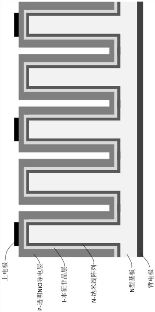
[0045] The back electrode has a thickness of 200nm and is made of metal aluminum;

[0046] N-type substrate, the thickness of which is 200 μm, the material is single crystal silicon, and nano-silver particles are deposited on the surface;

[0047] A nanowire cluster, the length of which is 1.8 μm, and the bottom diameter of each nanowire in the nanowire cluster is 190 nm;

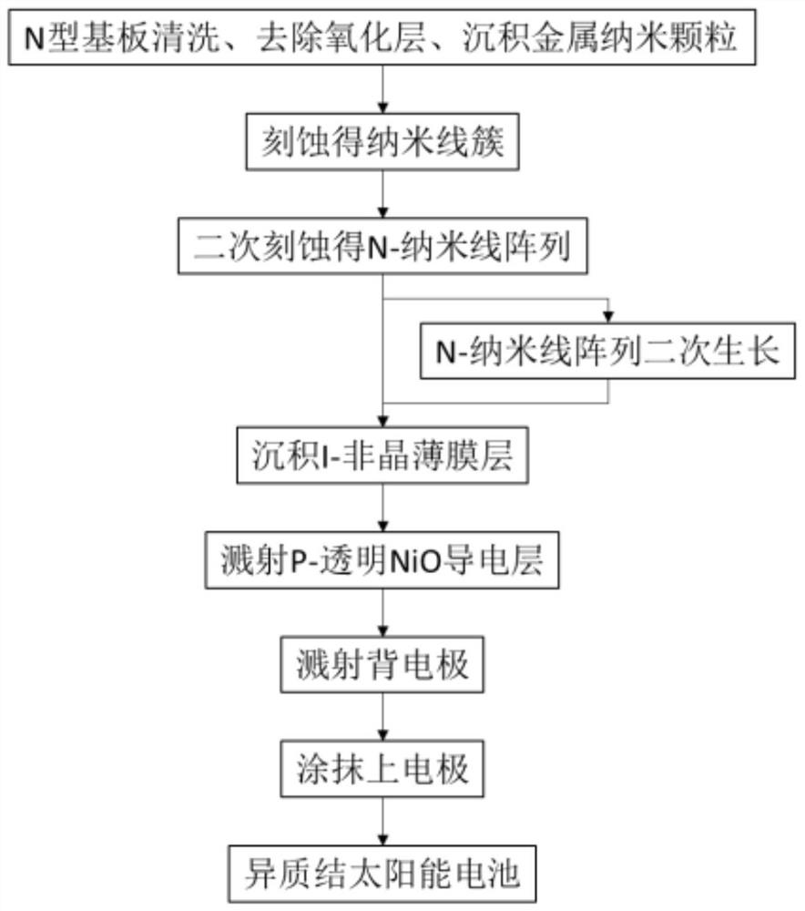
[0048]Using potassium hydroxide with a concentration of 10wt% and a pH of 15 to etch a second time for 10s, an N-nanowire array is obtained, wherein the length of each nanowire is 1 μm, and the diameter of the lower end surface is 190nm , The upper end is in the shape of a spherical crown, the diameter of the spherical bottom surface is 170nm, and the distance between adjacent nanowires is 100nm (between the lower end surface or the root);

[0049] I-intrinsic amorphous layer, its thickness is 70nm, material is germanium thin film;

[0050] P-transparent NiO conductive layer, its thickness is 140nm;

[0...

Embodiment 2

[0053] The back electrode has a thickness of 300nm and is made of metallic silver;

[0054] N-type substrate with a thickness of 300 μm, made of single crystal silicon, and deposited with nano-aluminum particles on the surface;

[0055] A nanowire cluster, the length of which is 2.0 μm, and the bottom diameter of each nanowire in the nanowire cluster is 205 nm;

[0056] N-nanowire arrays were obtained after secondary etching with sodium hydroxide with a concentration of 10wt% and a pH of 15 for 15 seconds, wherein the length of each nanowire was 1 μm, and the diameter of the lower end surface was 200 nm. , The upper end is in the shape of a spherical crown, the diameter of the spherical bottom surface is 170nm, and the distance between adjacent nanowires is 110nm (between the lower end surface or the root);

[0057] I-intrinsic amorphous layer, its thickness is 90nm, material is silicon thin film;

[0058] P-transparent NiO conductive layer, its thickness is 150nm;

[0059]...

Embodiment 3

[0061] The back electrode has a thickness of 200nm and is made of metal aluminum;

[0062] N-type substrate with a thickness of 200 μm, made of single crystal silicon, and deposited with nano-silver particles on the surface;

[0063] A nanowire cluster, the length of which is 1.8 μm, and the bottom diameter of each nanowire in the nanowire cluster is 190 nm;

[0064] After 15 seconds of secondary etching with potassium hydroxide with a concentration of 10wt% and a pH of 15, N-nanowire arrays were obtained by continuing PECVD regrowth, wherein the length of each nanowire was 1.2 μm, and the diameter of the lower end surface was 190 nm. , The upper end is in the shape of a spherical crown, the diameter of the spherical bottom surface is 110nm, and the distance between adjacent nanowires is 100nm (between the lower end surface or the root);

[0065] I-intrinsic amorphous layer, its thickness is 80nm, and material is germanium thin film;

[0066] P-transparent NiO conductive lay...


PUM

PropertyMeasurementUnit
lengthaaaaaaaaaa
lengthaaaaaaaaaa
diameteraaaaaaaaaa

Abstract

The invention provides a silicon heterojunction solar cell. The silicon heterojunction solar cell sequentially comprises a back electrode, an N type substrate, an N-nanowire array, an I-intrinsic amorphous layer, a P-transparent NiO conductive layer and an upper electrode, wherein the N-nanowire array is obtained by performing secondary etching on a nanowire cluster formed by etching on the basisof the N type substrate through an alkaline reagent, and comprises a plurality of nanowires which are not in contact with each other and have upper sharp parts and lower thick parts; and the N-nanowire array, the I-intrinsic amorphous layer and the P-transparent NiO conductive layer form a radial heterojunction. According to the solar cell, the cluster of the nanowire array is eliminated through secondary etching, and a phenomenon of lost due to that a large amount of incident sunlight is reflected by the nanowire cluster can be avoided on the premise that enough length is ensured; and in addition, passivation treatment on the nanowire array can be realized through the I-intrinsic amorphous layer, and the performance of the silicon heterojunction solar cell is ensured.

Description

technical field [0001] The invention relates to the technical field of batteries, in particular to a silicon heterojunction solar battery and a preparation method thereof. Background technique [0002] Due to the excellent optical and electrical properties of silicon nanowire arrays, silicon nanowire array cells have attracted extensive research, and various silicon nanowire array solar cells have emerged. Among them, the silicon nanowire radial heterojunction cell prepared by CVD method is a new type of solar cell developed by integrating nanotechnology, heterojunction technology, and thin film technology. development prospects. [0003] Silicon nanowire arrays have a good light trapping effect and can absorb more sunlight, but too long nanowires will collapse and cause obvious clusters, causing the incident light from the sun to be reflected and lost; too short nanowires to absorb sunlight The capacity is relatively limited, and the large surface area of ​​the nanowire a...

Claims


Application Information

Patent Timeline
Patent Type & Authority Patents(China)
IPC IPC(8): H01L31/0352H01L31/075H01L31/18
CPCH01L31/035227H01L31/075H01L31/1804Y02E10/547Y02E10/548Y02P70/50
Inventor 檀满林田勇郭震
Owner RESEARCH INSTITUTE OF TSINGHUA UNIVERSITY IN SHENZHEN
Learn More