Transmission electron microscope sample and method for producing same

A technology of electron microscope and manufacturing method, which is applied in the field of transmission electron microscope sample manufacture and transmission electron microscope sample, can solve the problem of indistinguishable silicon dioxide thin film, etc., and achieve the effect of easy measurement, clear interface and clear image

Inactive Publication Date: 2019-04-16
SHANGHAI HUALI INTEGRATED CIRCUTE MFG CO LTD
View PDF6 Cites 0 Cited by
  • Summary
  • Abstract
  • Description
  • Claims
  • Application Information

AI Technical Summary

Problems solved by technology

At this time, if the engineer needs to measure the thickness of different films or identify which film layer the particle defect is generated from, the ordinary TEM sample preparation method will not be able to meet this requirement, and the difference in contrast of the TEM image cannot distinguish between different doped oxides. Silicon films, such as figure 1 shown

Method used


Image

  • Transmission electron microscope sample and method for producing same
  • Transmission electron microscope sample and method for producing same
  • Transmission electron microscope sample and method for producing same

Examples


Embodiment 1

[0037] Transmission electron microscope (TEM) sample preparation method of the present invention comprises the following steps:

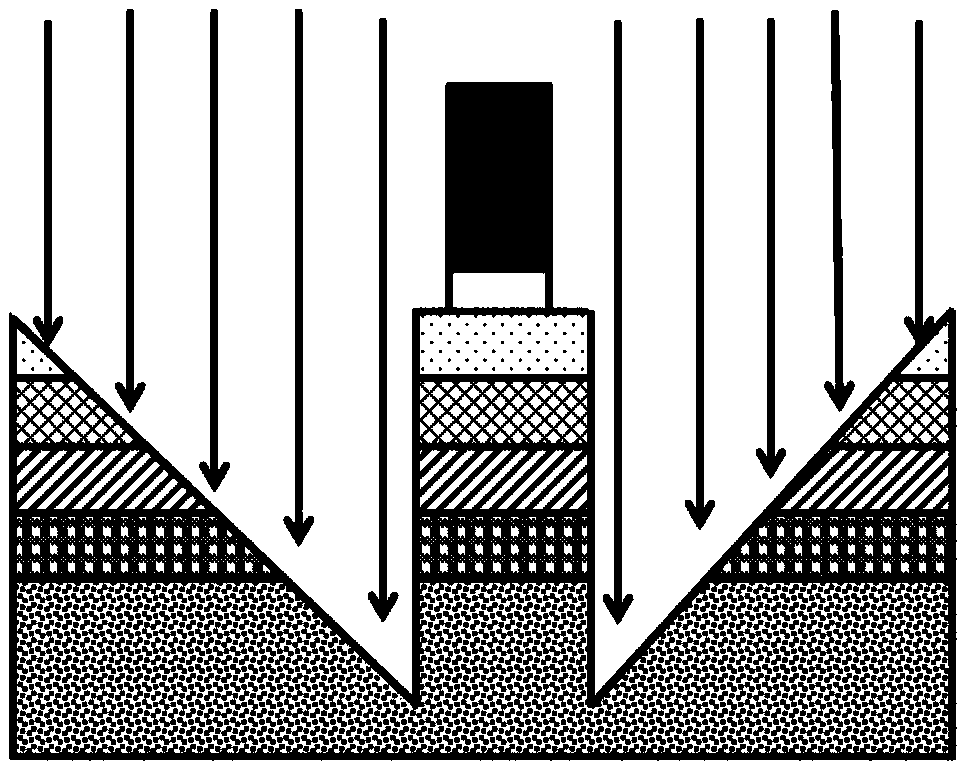
[0038] Step 1, put the sample into FIB (Focused Ion beam, focused ion beam), find the target area, deposit metal protection under E-Beam (electron beam, electron beam), I-Beam (Ion Beam, ion beam) layer. Focused ion beam technology (Focused Ion beam, FIB) is to use the electric lens to focus the ion beam into a very small ion beam bombarding the surface of the material, so as to realize the stripping, deposition, implantation, cutting and modification of the material. With the development of nanotechnology, nanoscale manufacturing industry is developing rapidly, and nanofabrication is the core part of nanomanufacturing industry. The representative method of nanofabrication is focused ion beam. Focused ion beam technology (FIB) uses high-intensity focused ion beams for nano-processing of materials, combined with scanning electron microscopes (SEM) a...

Embodiment 2

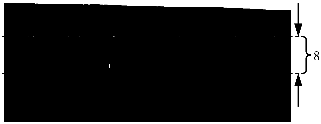
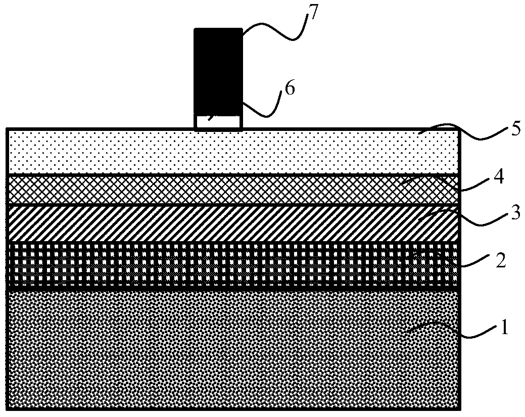
[0053] The invention also discloses a transmission electron microscope sample. The sample includes a silicon substrate, a polysilicon layer 2, a silicon nitride layer 3, a silicon dioxide thin film layer 4 grown based on a high aspect ratio process from bottom to top, and A doped silicate glass layer 5, an electron beam protection layer 6 and an ion beam protection layer 7; the non-doped silicate glass layer has a first thickness 9, and the silicon dioxide film grown based on a high aspect ratio process The layer has a second thickness 10, the silicon substrate, the polysilicon layer and the silicon nitride layer have a third thickness 11, and the values ​​of the first thickness 9, the second thickness 10 and the third thickness 11 are different. The difference range between the first thickness 9 and the second thickness 10 is between 10nm-100nm, and the difference range between the second thickness 10 and the third thickness 11 is also between 10nm-100nm.

[0054] The method ...


PUM


Abstract

The invention discloses a transmission electron microscope sample. The sample sequentially comprises a silicon substrate, a polycrystalline silicon layer, a silicon nitride layer, a silicon dioxide thin film layer grown on the basis of a high aspect ratio process, an undoped silicate glass layer, an electron beam protection layer and an ion beam protection layer from bottom to top, wherein the undoped silicate glass layer has a first thickness, the silicon dioxide thin film layer grown on the basis of the high aspect ratio process has a second thickness, the silicon substrate, the polycrystalline silicon layer and the silicon nitride layer have a third thickness, and the values of the first thickness, the second thickness and the third thickness are different from one another. The invention further discloses a manufacturing method of the transmission electron microscope sample. The transmission electron microscope sample prepared by the method disclosed by the invention can be used fordirectly obtaining thickness information of the silicon dioxide films grown in different growth modes through observation of images of the transmission electron microscope.

Description

technical field [0001] The present application relates to the field of semiconductor integrated circuits, in particular to a method for manufacturing a transmission electron microscope sample. The present application also relates to a transmission electron microscope sample. Background technique [0002] In the manufacture of semiconductor integrated circuits, silicon dioxide is an excellent insulating material, which is amorphous. The structure of silicon dioxide can be considered as four oxygen atoms located at the corners of a triangular polyhedron, and the center of the polyhedron is a silicon atom. In this way, every 4 oxygen atoms are approximately covalently bonded to silicon atoms, satisfying the valence shell of silicon. Silicon dioxide generally does not react with water, that is, it does not generate silicic acid in contact with water. Because silicon dioxide has extremely stable chemical properties, it can be used as a gap between the upper and lower metal layer...

Claims


Application Information

Patent Timeline
IPC IPC(8): G01N23/2202
CPCG01N23/2202G01N2223/07G01N2223/61G01N2223/633
Inventor 袁安东
Owner SHANGHAI HUALI INTEGRATED CIRCUTE MFG CO LTD
Why Eureka
Try Eureka