Optical module and welding method thereof

A welding method and technology for optical modules, applied in the field of optical modules, can solve problems such as large jitter, influence effect, overshoot, etc., and achieve the effects of improving the return path, improving performance, and optimizing impedance continuity.

Inactive Publication Date: 2019-04-16
HISENSE BROADBAND MULTIMEDIA TECH
View PDF4 Cites 8 Cited by
  • Summary
  • Abstract
  • Description
  • Claims
  • Application Information

AI Technical Summary

Problems solved by technology

[0002] The demand of the communication market has been promoting the improvement of the basic transmission rate of optical communication, and the improvement of the basic transmission rate of the photoelectric conversion module depends to a large extent on the performance of the optical device itself and the driving ability of the driving chip; among them, with the signal With the improvement of the transmission rate, the integrity of the electrical signal has been raised to a new level. As the single-channel signal transmission rate is increased to 25G, the optical m

Method used


Image

  • Optical module and welding method thereof
  • Optical module and welding method thereof
  • Optical module and welding method thereof

Examples


Embodiment Construction

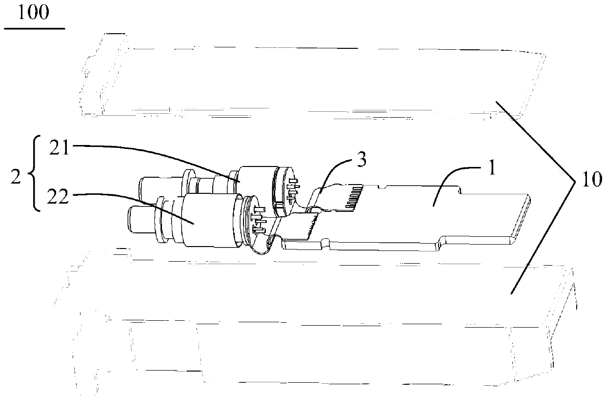
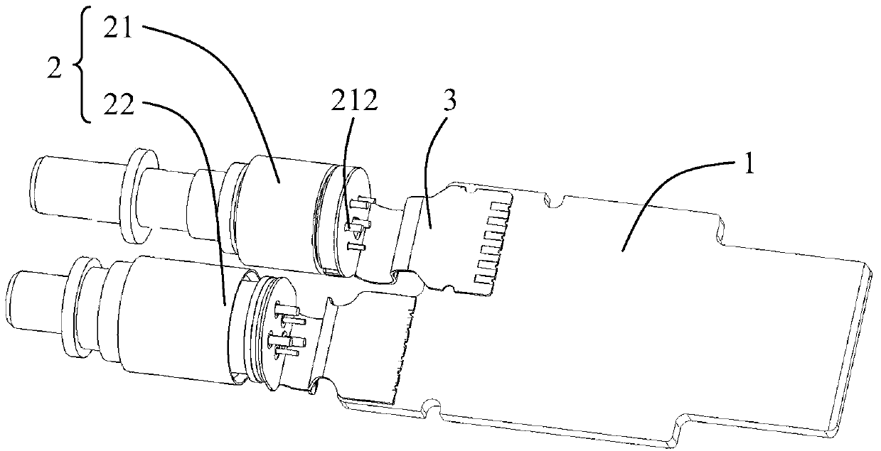
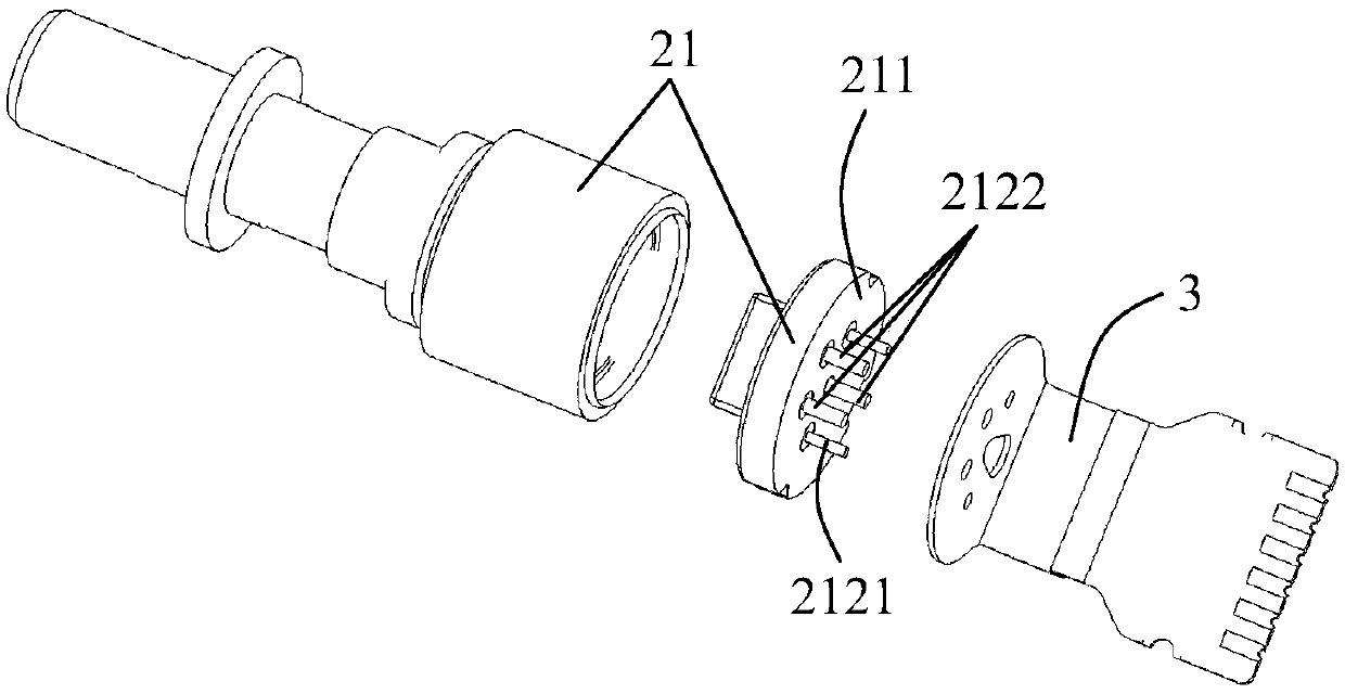
[0021] The present invention will be described in detail below in conjunction with specific embodiments shown in the accompanying drawings. However, these embodiments do not limit the present invention, and any structural, method, or functional changes made by those skilled in the art according to these embodiments are included in the protection scope of the present invention.

[0022] The terminology used in the present invention is for the purpose of describing particular embodiments only and is not intended to limit the invention. As used herein and in the appended claims, the singular forms "a", "the", and "the" are intended to include the plural forms as well, unless the context clearly dictates otherwise. It should also be understood that the term "and / or" as used herein refers to and includes any and all possible combinations of one or more of the associated listed items.

[0023] Some embodiments of the present invention will be described in detail below with referenc...


PUM


Abstract

The invention discloses an optical module and a welding method thereof. The optical module comprises a PCB, an optoelectronic component and a flexible circuit board which is connected with the PCB andthe optoelectronic component; wherein the optoelectronic component comprises a light emitting assembly, the light emitting assembly comprises a matching surface which is connected with the flexible circuit board in a matched mode, and an electric connecting part is arranged on the matching surface; the flexible circuit board comprises a bonding pad region which is adapted to the matching surface,the bonding pad region is provided with a grounding bonding pad used for being connected with the electrical connection portion, and a conductive region electrically connected with the grounding bonding pad, the conductive region is arranged on the side, opposite to the matching surface, of the flexible circuit board and is electrically fixed on the matching surface. According to the method, theconductive region is arranged on the flexible circuit board which is connected with the light emitting assembly in the optoelectronic component, so that comprehensive welding can be achieved between the flexible circuit board and the matching surface of the emitting light assembly, so that the backflow path of the high-speed signal is improved, the impedance continuity of the high-speed line is optimized, and the performance of the transmitting end eye diagram of the optical module is improved.

Description

technical field [0001] The invention relates to the technical field of optical modules, in particular to an optical module and a welding method thereof. Background technique [0002] The demand of the communication market has been promoting the improvement of the basic transmission rate of optical communication, and the improvement of the basic transmission rate of the photoelectric conversion module depends to a large extent on the performance of the optical device itself and the driving ability of the driving chip; among them, with the signal With the improvement of the transmission rate, the integrity of the electrical signal has been raised to a new level. As the single-channel signal transmission rate is increased to 25G, the optical module design has increasingly stringent requirements for PCB (Printed Circuit Board, printed circuit board) wiring. For If the impedance matching of the high-speed signal line design is not perfect, it will greatly affect the effect of opt...

Claims


Application Information

Patent Timeline
IPC IPC(8): G02B6/42
CPCG02B6/4202G02B6/4281
Inventor 陈彪
Owner HISENSE BROADBAND MULTIMEDIA TECH
Why Eureka
Try Eureka