
TFT array substrate board and alignment method thereof

An array substrate, alignment mark technology, applied in optics, instruments, electrical components, etc., can solve the problem of low success rate of alignment marks 200, and achieve the effect of improving the success rate of grabbing and reducing the rate of false grabbing

Inactive Publication Date: 2019-04-16
SHENZHEN CHINA STAR OPTOELECTRONICS SEMICON DISPLAY TECH CO LTD
View PDF6 Cites 8 Cited by
  • Summary
  • Abstract
  • Description
  • Claims
  • Application Information

AI Technical Summary

Problems solved by technology

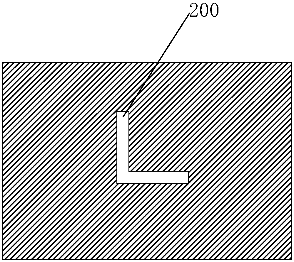
like figure 1 As shown, the existing TFT array substrate etches a hollow "L"-shaped blank area (also called headroom), the "L"-shaped blank area is used as the alignment mark 200, when the alignment device actually grabs the alignment mark 200, because the four corners of the alignment mark 200 are similar to the characteristics of "L", when the alignment When the positioning equipment scans and grabs the alignment mark 200 with an electron gun, the junction position between the four corners of the alignment mark 200 and the glass substrate will cause interference when the alignment equipment captures the features of the alignment mark 200, and this interference will affect the alignment equipment. Take the alignment mark 200, and the alignment mark 200 appears white in the alignment equipment, and the surrounding features of the alignment mark 200 also appear white, resulting in the equipment grabbing the alignment mark 200, which cannot effectively identify the captured "L" Whether the shape alignment mark 200 is correct, the entire alignment mark 200 is shifted when the alignment equipment grabs it, and the success rate of grabbing the alignment mark 200 is not high

Method used


Image

  • TFT array substrate board and alignment method thereof
  • TFT array substrate board and alignment method thereof
  • TFT array substrate board and alignment method thereof

Examples


Embodiment Construction

[0027] In order to further illustrate the technical means adopted by the present invention and its effects, the following describes in detail in conjunction with preferred embodiments of the present invention and accompanying drawings.

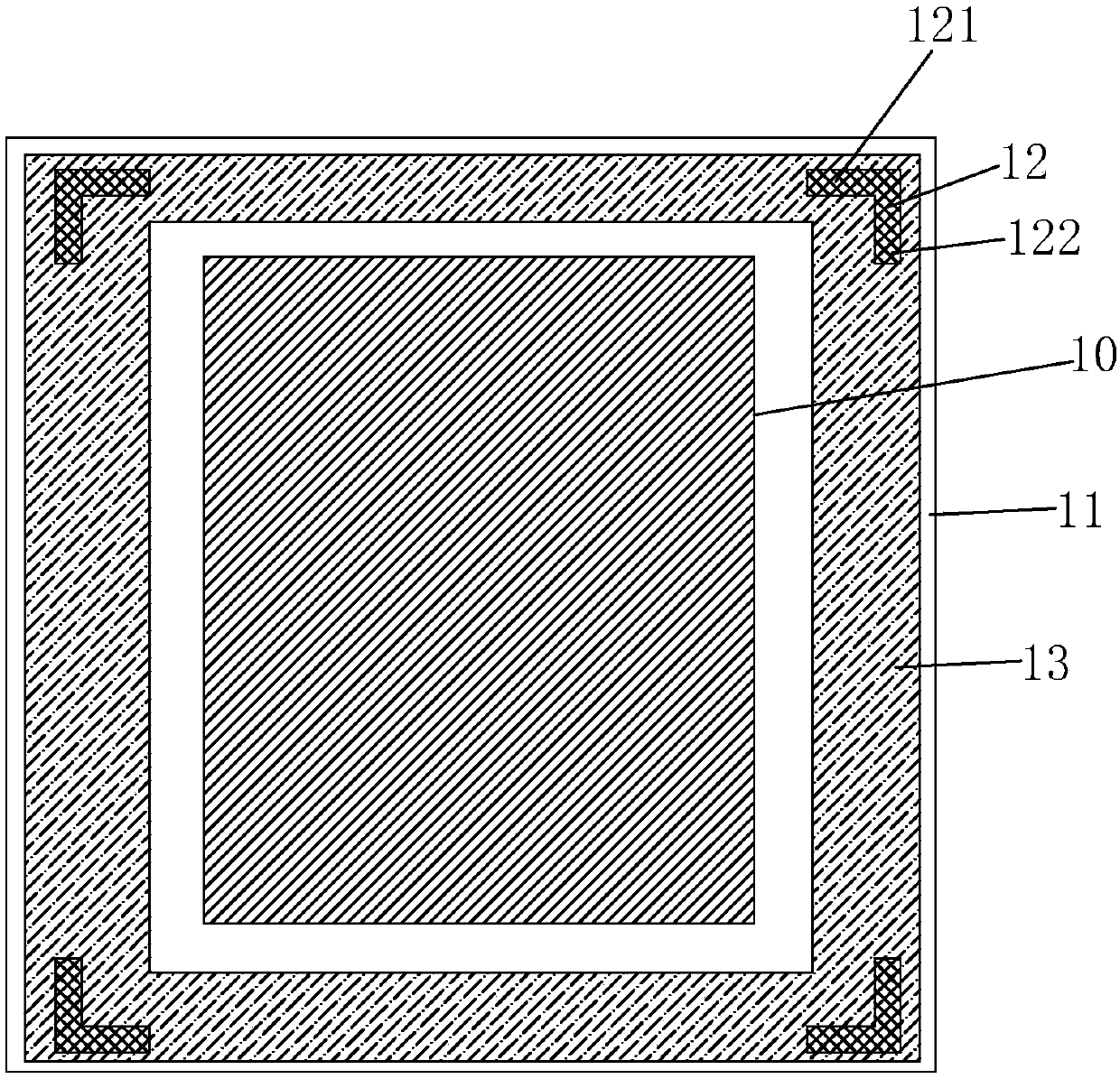
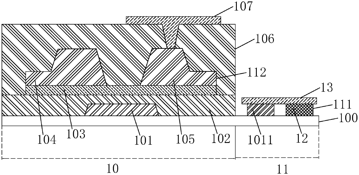
[0028] see Figure 2 to Figure 4 , the present invention provides a TFT array substrate, comprising: a display area 10 and a non-display area 11 surrounding the display area 10; an alignment mark 12 is provided on the non-display area 11 and an alignment mark 12 The transparent conductive layer 13 on and in contact with the alignment mark 12.

[0029] It should be noted that, in the present invention, a transparent conductive layer 13 in contact with the alignment mark 12 is provided on the alignment mark 12. The ability of layer 13 to bind electrons is different, so that the alignment mark 12 appears black in the alignment equipment, and the transparent conductive layer 13 appears gray in the alignment equipment, forming an obvious grayscale...


PUM


Abstract

The invention provides a TFT array substrate board and an alignment method thereof. The TFT array substrate board comprises a display area and a non-display area surrounding the display area, whereinthe non-display area is provided with alignment marks and a transparent conducting layer which is arranged on the alignment marks and is in contact with the alignment marks; when alignment equipment scans the area where the alignment marks are located through electronic scanning, the different bound electron capacity of the alignment marks and the transparent conducting layer are used to enable the alignment marks to show black in the alignment equipment, the transparent conducting layer is in grey color in the alignment equipment, and obvious grey-scale comparison is formed, the grabbing success rate of alignment marks is improved, and the false grabbing rate of alignment equipment is reduced

Description

technical field [0001] The invention relates to the field of display technology, in particular to a TFT array substrate and an alignment method thereof. Background technique [0002] Thin Film Transistor (TFT) is the main driving element in current Liquid Crystal Display (LCD) and Active Matrix Organic Light-Emitting Diode (AMOLED). It is related to the display performance of the flat panel display device. [0003] Most of the liquid crystal displays currently on the market are backlight liquid crystal displays, which include a liquid crystal display panel and a backlight module. The working principle of the liquid crystal display panel is to pour liquid crystal molecules between the thin film transistor array substrate (ThinFilm Transistor Array Substrate, TFT Array Substrate) and the color filter (ColorFilter, CF) substrate, and apply pixel voltage on the two substrates respectively. and the common voltage, through the electric field formed between the pixel voltage and ...

Claims


Application Information

Patent Timeline
Patent Type & Authority Applications(China)
IPC IPC(8): G02F1/1333H01L23/544H01L27/12
CPCG02F1/1333G02F1/133354H01L23/544H01L27/1214H01L2223/54426
Inventor 刘强
Owner SHENZHEN CHINA STAR OPTOELECTRONICS SEMICON DISPLAY TECH CO LTD
Learn More