Method for monitoring semiconductor device STI shape, application method thereof, and method for improving TCR structure

A semiconductor and device technology, which is applied in the field of improving TCR structure and STI morphology monitoring of semiconductor devices, and can solve the problems of process error detection, monitoring equipment and monitoring methods, large leakage current of semiconductor devices, and inability to accurately monitor characteristic parameters, etc.

Active Publication Date: 2019-04-16
SHANGHAI HUALI INTEGRATED CIRCUTE MFG CO LTD
View PDF4 Cites 2 Cited by
  • Summary
  • Abstract
  • Description
  • Claims
  • Application Information

AI Technical Summary

Problems solved by technology

[0003] However, in the manufacturing process of semiconductor devices, due to various process errors, improper detection and monitoring equipment and monitoring methods, various characteristic parameters in the manufacturing proc

Method used


Image

  • Method for monitoring semiconductor device STI shape, application method thereof, and method for improving TCR structure
  • Method for monitoring semiconductor device STI shape, application method thereof, and method for improving TCR structure
  • Method for monitoring semiconductor device STI shape, application method thereof, and method for improving TCR structure

Examples


Embodiment Construction

[0025] The technical solutions in the present invention will be clearly and completely described below in conjunction with the accompanying drawings. Apparently, the described embodiments are part of the embodiments of the present invention, not all of them. Based on the embodiments of the present invention, all other embodiments obtained by persons of ordinary skill in the art without making creative efforts belong to the protection scope of the present invention.

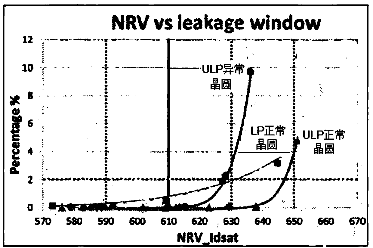
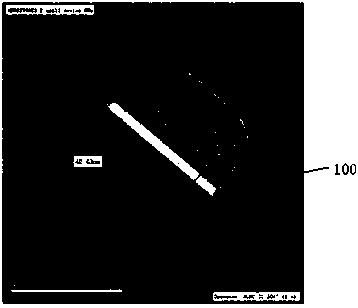
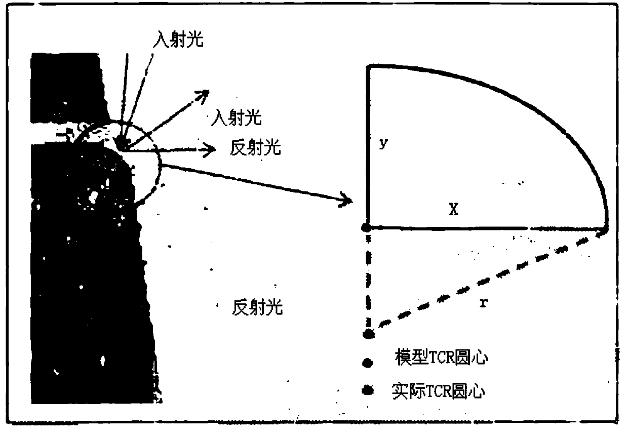
[0026] The semiconductor device involved in the invention is an ultra-low power consumption product (ULP); in addition, the semiconductor device involved in the invention includes shallow trench isolation etching (STI) silicon in an active region. Compared with ordinary low-power products (LP), ultra-low-power products (ULP) increase the top corner rounding (TCR) structure of the silicon material in the STI active area, which effectively reduces the leakage current . Specifically, see figure 2 , figure 2 It i...


PUM


Abstract

The invention relates to a method for monitoring the shallow trench isolation etching shape of a semiconductor device, and relates to the technical field of microelectronics. The method includes stepsof S1, collecting the actual measurement spectrum of the semiconductor device for semiconductor device STI structures with different etching times by using an optical line width measuring instrument;S2: modeling and defining the theoretical model structure of a TCR structure; S3, slice determining the actual data of the TCR structure; S4, according to the actual measurement spectrum collected inthe step S1 and the theoretical model structure in the step S2, obtaining the measurement program library file of the TCR structure by further analysis and calculation; S5: collecting the theoreticaldata of the parameters of the TCR structure to be monitored by using the measurement program library file, and establishing a relationship between the theoretical data and the actual data collected in the step S3, and determining a correlation coefficient R2 of the theoretical data and the actual data; S6, obtaining the parameters of the TCR structure by using the correlation coefficient R2 and the measurement program library file obtained in the step S4. The method monitors the TCR structure shape, and achieves a purpose of stabilizing the shallow trench TCR structure process.

Description

technical field [0001] The invention relates to the technical field of microelectronics, in particular to a method for monitoring the STI shape of a semiconductor device, an application method thereof and a method for improving a TCR structure. Background technique [0002] In the field of microelectronics technology, the saturation current of a semiconductor device is an important parameter of the semiconductor device, and it is generally desired that the saturation current of the semiconductor device be as large as possible. [0003] However, in the manufacturing process of semiconductor devices, due to various process errors, improper detection and monitoring equipment and monitoring methods, various characteristic parameters in the manufacturing process of semiconductor devices cannot be accurately monitored, and thus cannot be effectively improved, resulting in semiconductor The device cannot meet the demand, such as the leakage current of the semiconductor device is re...

Claims


Application Information

Patent Timeline
IPC IPC(8): H01L21/66G06F17/50
CPCG06F30/20H01L22/12H01L22/20
Inventor 冯奇艳吴智勇
Owner SHANGHAI HUALI INTEGRATED CIRCUTE MFG CO LTD
Why Eureka
Try Eureka