Preparation method of compound semiconductor thin film solar cell

A solar cell and semiconductor technology, applied in the field of solar cells, can solve the problems of low battery open circuit voltage and large battery open voltage loss, and achieve the effects of improving device efficiency and open circuit voltage, which is beneficial to commercialization and application.

Inactive Publication Date: 2019-04-16
NANKAI UNIV
View PDF5 Cites 6 Cited by
  • Summary
  • Abstract
  • Description
  • Claims
  • Application Information

AI Technical Summary

Problems solved by technology

[0003] At present, the main factor limiting the conversion efficiency of CZTSSe thin film solar cells is that the cell has a large open voltage loss, which makes the open circuit voltage of the cell low.

Method used


Image

  • Preparation method of compound semiconductor thin film solar cell
  • Preparation method of compound semiconductor thin film solar cell
  • Preparation method of compound semiconductor thin film solar cell

Examples


Embodiment Construction

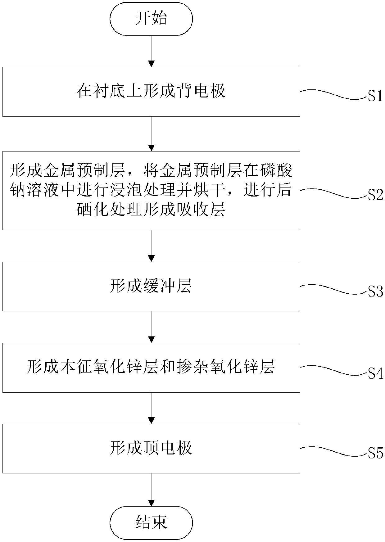
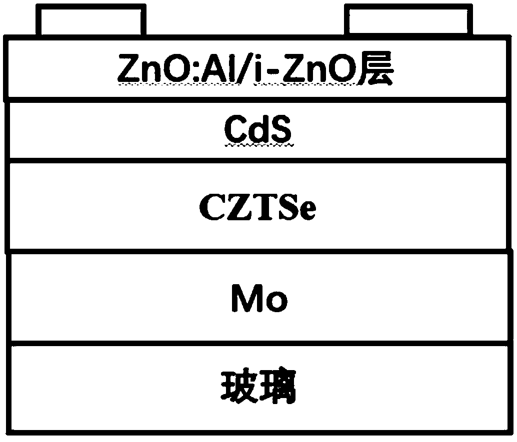
[0018] In order to make the objectives, technical solutions and advantages of the present invention clearer, the following will clearly and completely describe the technical solutions in the embodiments of the present invention with reference to the accompanying drawings in the embodiments of the present invention. It should be understood that the specifics described here The examples are only used to explain the present invention, but not to limit the present invention. The described embodiments are only a part of the embodiments of the present invention, rather than all the embodiments. Based on the embodiments of the present invention, all other embodiments obtained by those of ordinary skill in the art without creative work shall fall within the protection scope of the present invention.

[0019] In the description of the present invention, it should be noted that the orientation or positional relationship indicated by the terms "upper", "lower", "vertical", "horizontal", etc...


PUM

PropertyMeasurementUnit
thicknessaaaaaaaaaa
thicknessaaaaaaaaaa
thicknessaaaaaaaaaa

Abstract

The invention discloses a preparation method of a compound semiconductor thin film solar cell. The preparation method comprises the following steps of forming a back electrode, in which the back electrode is formed on a substrate; forming an absorption layer, in which a metal pre-fabrication layer is formed on on the back electrode, the metal pre-fabrication layer is immersed in a Na3PO4 solutionand is processed and dried, and post-selenylation is performed on the dried metal pre-fabrication layer to form the absorption layer; forming a buffer layer, in which the buffer layer is formed on theabsorption layer; forming a window layer, in which an intrinsic zinc oxide layer and a doping zinc oxide layer are formed on the buffer layer; and forming a top electrode, in which the top electrodeis formed on the window layer. The metal pre-fabrication layer is processed by the Na3PO4 solution, so that the open-circuit voltage of the compound semiconductor thin film solar cell is remarkably improved, and the device efficiency can be obviously improved; and moreover, the preparation method is low in cost and is beneficial for market promotion and application.

Description

Technical field [0001] The invention relates to the technical field of solar cells, in particular to a method for preparing compound semiconductor thin film solar cells. Background technique [0002] Solar energy is the most ideal renewable energy in the future due to its advantages such as wide distribution, clean and pollution-free, abundant resources, and inexhaustible. Solar photovoltaic power generation is the most attractive solution to utilize solar energy resources. The main problem that photovoltaic power generation currently needs to solve is the production cost of solar cells and the efficiency of the cells. Compound semiconductor thin film solar cells have great advantages in commercial applications due to their excellent power generation performance, lower materials and energy consumption. Among them, copper indium gallium selenide (CIGS) and cadmium telluride (CdTe) and other compound semiconductor thin-film batteries containing rare metals and toxic elements have...

Claims


Application Information

Patent Timeline
Patent Type & Authority Applications(China)
IPC IPC(8): H01L31/0445H01L31/18
CPCH01L31/0445H01L31/18Y02E10/50Y02P70/50
Inventor 张毅王东潇高守帅武莉
Owner NANKAI UNIV
Why Eureka
Try Eureka