Unlock instant, AI-driven research and patent intelligence for your innovation.

A CMOS output driving circuit with feedback control

An output drive circuit, feedback control technology, applied in the direction of reliability improvement and modification, etc., can solve the problems of reducing noise tolerance, affecting logic level, reducing circuit speed, etc., to reduce power supply bounce noise, reduce bounce noise, output Effect of Transient Current Reduction

Active Publication Date: 2019-05-03
BEIJING MXTRONICS CORP +1
View PDF7 Cites 0 Cited by
  • Summary
  • Abstract
  • Description
  • Claims
  • Application Information

AI Technical Summary

Problems solved by technology

Deviations in internal supply voltages affect logic levels and reduce noise margins
[0003] The traditional slope control circuit, while reducing the noise of the power supply, increases the delay of the circuit, resulting in a decrease in the corresponding speed of the circuit

Method used


Image

  • A CMOS output driving circuit with feedback control
  • A CMOS output driving circuit with feedback control
  • A CMOS output driving circuit with feedback control

Examples


Embodiment Construction

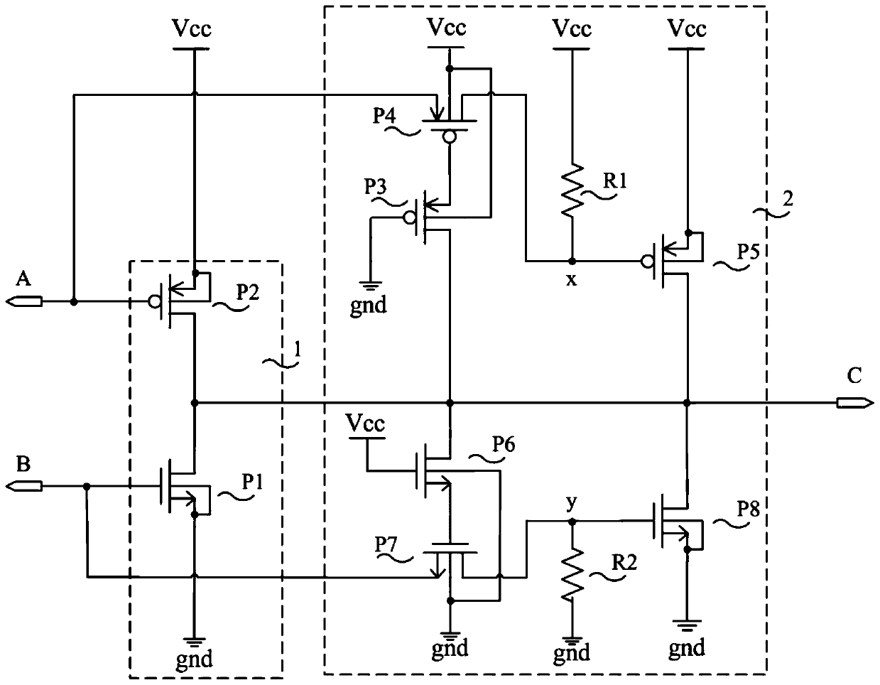
[0028] Such as figure 1 Shown is a structural diagram of a CMOS output drive circuit with feedback control in the present invention, including a CMOS drive circuit 1 and a feedback control circuit 2 . The CMOS drive circuit 1 includes an NMOS transistor P1 and a PMOS transistor P2, and the feedback control circuit 2 includes a PMOS transistor P3, a PMOS transistor P4, a PMOS transistor P5 and a resistor R1.

[0029] The MOS tubes used in the present invention are all enhanced MOS tubes.

[0030] The input signal of input port A and input port B has three states, at the same time high level, output C is low level; at the same time low level, output C is high level; input port A is high level, input port B is low level, and output C is high impedance state at this time.

[0031] The CMOS drive circuit controls the NMOS transistor P1 and the PMOS transistor P2 to be turned on alternately through the input port A and the input port B to realize the high and low level driving of...


PUM


Abstract

The invention discloses a CMOS output driving circuit with feedback control. The CMOS output driving circuit comprises a CMOS driving circuit and a feedback control circuit. The feedback circuit comprises an MOS tube which is used for device protection and is in a normally-on state, an MOS tube which controls the on / off state of a feedback loop, an auxiliary driving MOS tube and an RC (Resistor-Capacitor) charging / discharging circuit which is composed of a resistor and an auxiliary driving MOS tube gate capacitor. The circuit is used in a CMOS device output driving circuit, and is characterized in that the slope of a device output signal is controlled through a feedback loop, and the transmission delay of the device is not affected as much as possible while the slope of the output signal is reduced.

Description

technical field [0001] The present invention relates to a CMOS output drive circuit with feedback control, in particular, when the device outputs a high-level signal, the circuit can ensure a faster signal slope at the output terminal before establishing an effective high logic level, During the period when the output terminal reaches an effective high logic level and continues to rise to the power supply voltage, reducing the slope of the output signal and reducing the transient current belongs to the field of device control. Background technique [0002] see figure 2 , during each switching process of the output of the integrated circuit, the transient current flowing into the power supply rail charges or discharges the circuit capacitance, no matter the VDD or VSS connection of the chip is connected to the external power supply through the bonding wire and the package lead , thus having a non-negligible series inductance. Therefore, the transient current change will gen...

Claims


Application Information

Patent Timeline
IPC IPC(8): H03K19/003
CPCY02B70/10
Inventor 王帆刘玉清赵玉姣麻军野李建成陈莉明陈茂鑫宋小敬王佳时飞刘志刚
Owner BEIJING MXTRONICS CORP