Stacked backside illuminated spad array

A back-illuminated, wafer-based technology, applied in the field of stacked back-illuminated SPAD arrays, can solve problems such as reducing the timing resolution or response time of the SPAD area, increasing the power consumption of the SPAD image sensor, and high breakdown voltage.

Active Publication Date: 2019-05-03
APPLE INC
View PDF11 Cites 6 Cited by
  • Summary
  • Abstract
  • Description
  • Claims
  • Application Information

AI Technical Summary

Problems solved by technology

Thicker semiconductor wafers increase photon detection efficiency in the SPAD region, but thicker semiconductor wafers may reduce the timing resolution or response time of the SPAD region because charge carriers must propagate through the thicker semiconductor wafer
In addition, thicker semiconductor wafers can lead to higher breakdown voltage, which increases the power consumption of the SPAD image sensor when the SPAD image sensor operates in Geiger mode

Method used


Image

  • Stacked backside illuminated spad array
  • Stacked backside illuminated spad array
  • Stacked backside illuminated spad array

Examples


Embodiment Construction

[0027] Reference will now be made in detail to the representative embodiments illustrated in the accompanying drawings. It should be understood that the following description is not intended to limit the embodiments to one preferred embodiment. On the contrary, it is intended to cover alternatives, modifications and equivalents, which may be included within the spirit and scope of the described embodiments as defined by the appended claims.

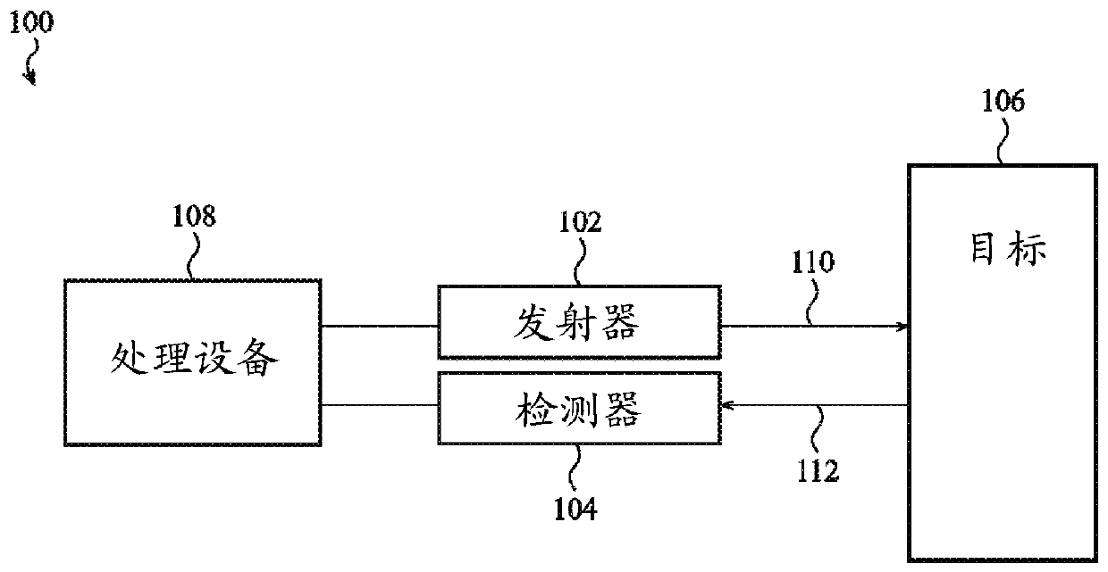
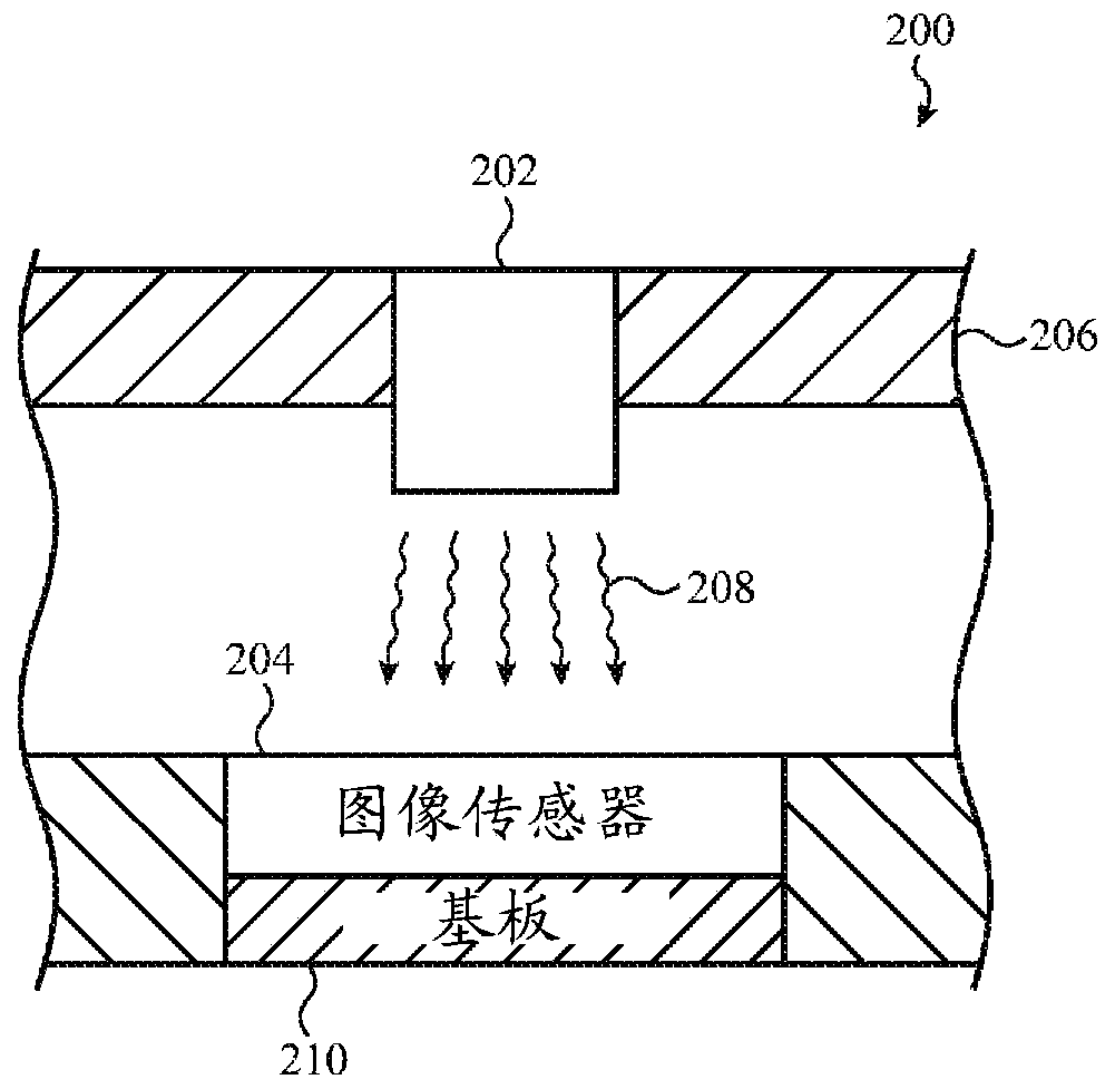
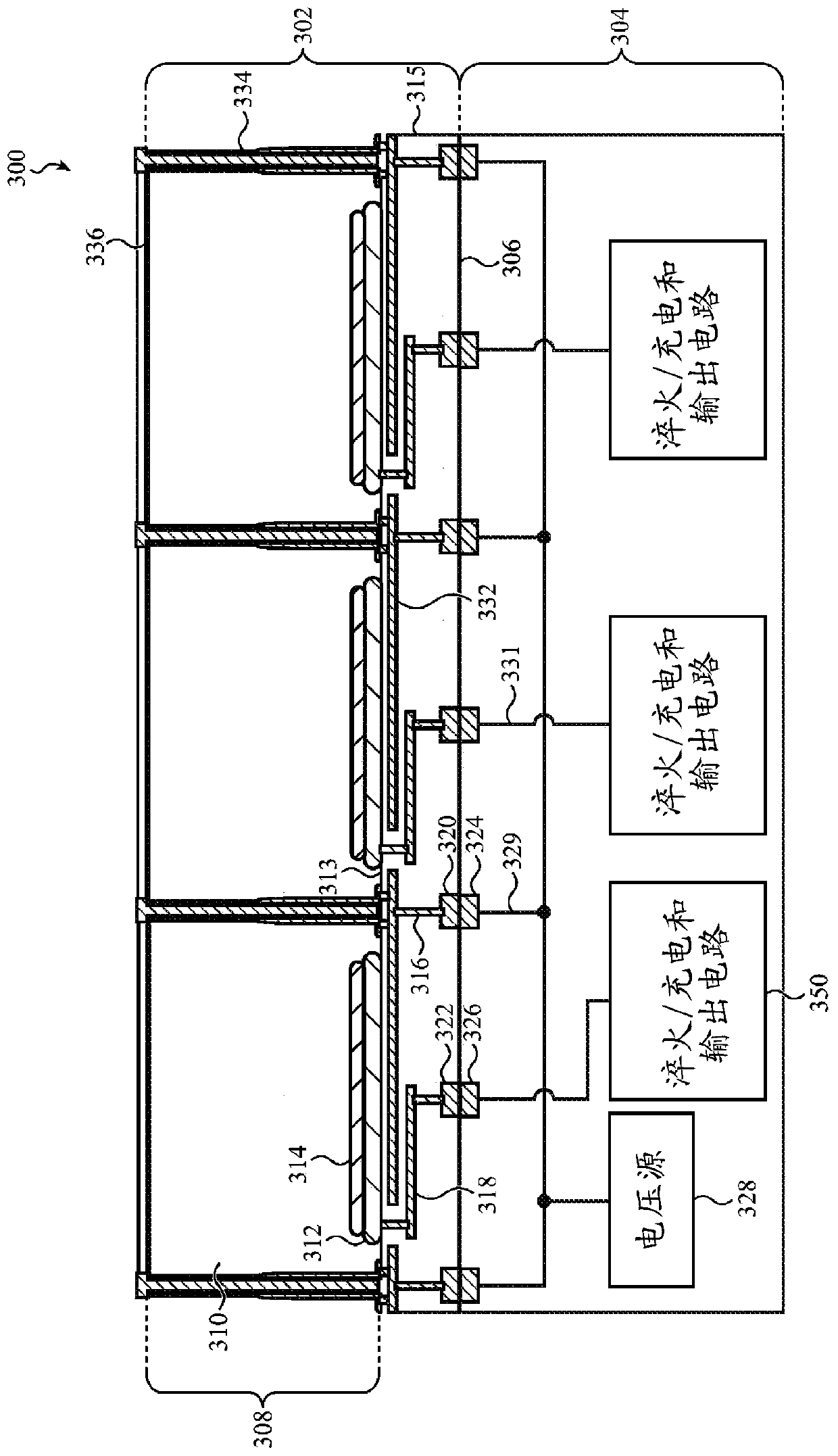
[0028] The following disclosure relates to back-illuminated single photon avalanche diode SPAD image sensors. A SPAD image sensor includes a sensor wafer and a separate circuit wafer attached or bonded to the front surface of the sensor wafer. A sensor wafer includes one or more SPAD regions. Each SPAD region includes a photosensitive semiconductor portion and functions as a pixel element of the SPAD image sensor, ie it receives photons and generates an electric current. The semiconductor portion of each SPAD is configured as a diode. ...


PUM


Abstract

A back-illuminated single-photon avalanche diode (SPAD) image sensor includes a sensor wafer stacked vertically over a circuit wafer. The sensor wafer includes one or more SPAD regions, with each SPADregion (400) including an anode gradient layer (402), a cathode region (404) positioned adjacent to a front surface of the SPAD region, and an anode avalanche layer (408) positioned over the cathoderegion. Each SPAD region is connected to a voltage supply and an output circuit in the circuit wafer through inter-wafer connectors. Deep trench isolation elements (424) are used to provide electricaland optical isolation between SPAD regions.

Description

[0001] Cross References to Related Applications [0002] This PCT patent application claims U.S. Provisional Patent Application 62 / 398,712, filed September 23, 2016, entitled "Back-Illuminated SPAD Image Sensor," and the title The contents of both applications are hereby incorporated by reference in their entirety, as the priority of US Provisional Patent Application 62 / 398,709 for "Back-Illuminated SPAD Image Sensor." technical field [0003] The embodiments generally relate to single photon avalanche diode SPAD image sensors. Background technique [0004] Image sensors are used in a variety of electronic devices, such as digital cameras, cellular telephones, copiers, medical imaging equipment, security systems, and time-of-flight cameras. Image sensors typically include an array of photodetectors that detect or respond to incident light. One type of photodetector that can be used in image sensors is the single photon avalanche diode (SPAD) region. The SPAD region is a p...

Claims


Application Information

Patent Timeline
Patent Type & Authority Applications(China)
IPC IPC(8): H01L27/146G01S7/4861G01S7/4863
CPCH01L27/1464H01L27/14629H01L27/14616H01L27/14623H01L27/1463H01L27/14643H01L27/14665H01L27/1461H01L27/14634H01L27/14632H01L27/14603H01L27/14627H01L31/107G01S7/4863H01L27/14609H04N25/75H04N25/587H04N25/617H04N25/709H04N25/745H04N25/771G01S7/4861H01L31/02027H01L31/03529
Inventor 万代新悟C·L·尼克拉斯N·卡拉萨瓦范晓峰A·拉弗莱奎尔G·A·阿格拉诺弗
Owner APPLE INC
Why Eureka
Try Eureka