Semiconductor wafer processing device and semiconductor wafer processing method

A processing device and processing method technology, applied in semiconductor/solid-state device manufacturing, electrical components, circuits, etc., can solve problems such as failure to sense the normal distribution of liquid medicine in time, etching without normal distribution of liquid medicine, and inability to make improvements in time. , to avoid poor etching, simple structure and low cost

Active Publication Date: 2021-01-26
CHANGXIN MEMORY TECH INC
View PDF6 Cites 0 Cited by
  • Summary
  • Abstract
  • Description
  • Claims
  • Application Information

AI Technical Summary

Problems solved by technology

[0003] In view of the above-mentioned shortcomings of the prior art, the object of the present invention is to provide a semiconductor wafer processing device and a semiconductor wafer processing method, which are used to solve the problems caused by the inability to detect whether the liquid medicine is normally distributed in the prior art. The problem that improvement measures cannot be taken in time when the liquid is not distributed normally and causes problems such as poor etching

Method used


Image

  • Semiconductor wafer processing device and semiconductor wafer processing method
  • Semiconductor wafer processing device and semiconductor wafer processing method
  • Semiconductor wafer processing device and semiconductor wafer processing method

Examples


Embodiment 2

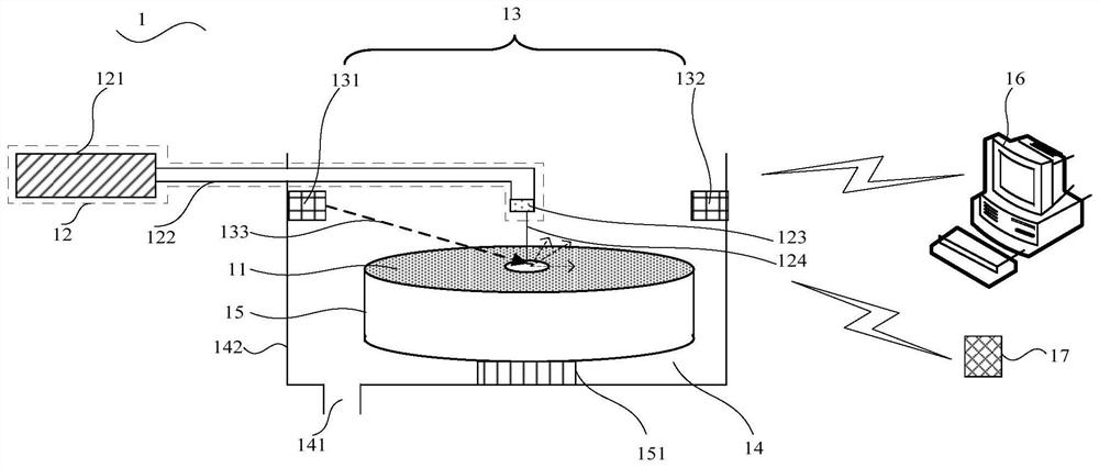
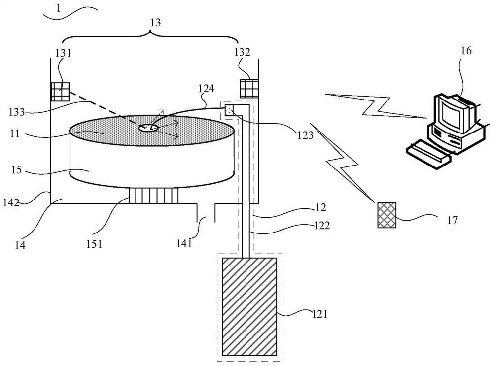
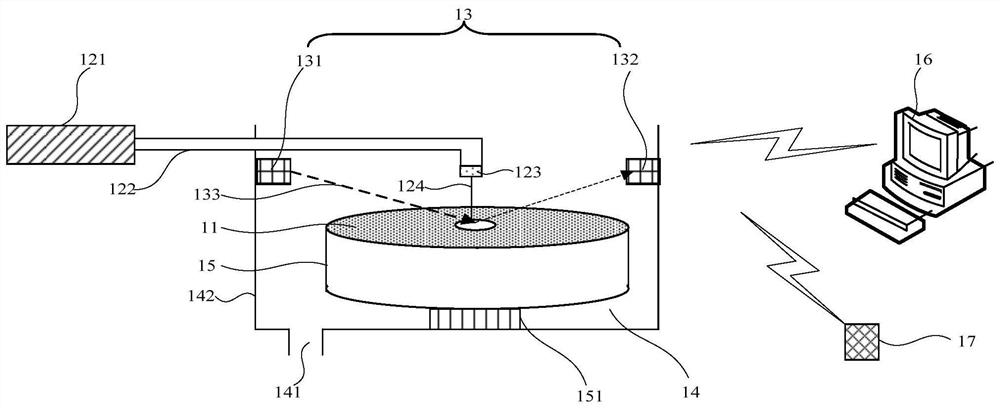
[0055] Such as Figure 5 Shown, the present invention also provides a kind of semiconductor wafer processing method, described semiconductor wafer processing method comprises the steps:

[0056] 1) providing a semiconductor wafer 11;

[0057] 2) Use the semiconductor wafer processing apparatus 1 as described in Embodiment 1 to spray the processing liquid 124 on the upper surface of the semiconductor wafer 11 and detect the distribution of the surface processing liquid 124 on the semiconductor wafer 11 .

[0058] Specifically, the detailed steps of the semiconductor wafer processing method may be as follows: S11, providing a semiconductor wafer 11, placing the semiconductor wafer 11 in the semiconductor wafer processing device 1 as described in Embodiment 1, More specifically, place it on the carrying table 15 and set the spraying time; then proceed to step S12, spray the processing liquid 124 on the surface of the semiconductor wafer 11 through the liquid supply system 12, at...


PUM


Abstract

The invention provides a semiconductor wafer processing device and a semiconductor wafer processing method. The semiconductor wafer processing device includes a carrier table, a liquid supply system and a detection sensor; the carrier table is used to carry the wafer; the liquid supply system includes a liquid source and a liquid supply pipeline for spraying processing liquid on the surface of the wafer; the detection sensor includes The transmitting module and the receiving module are located above the carrying platform and are used to detect the distribution of the wafer surface treatment liquid. The use of the semiconductor wafer processing device of the present application can promptly detect the poor distribution of the processing liquid, avoiding problems such as poor etching, poor development, and poor cleaning caused by uneven distribution of the processing liquid, thereby helping production personnel to timely address the distribution of the processing liquid. To solve the problem of unevenness, make improvement countermeasures to improve production yield. The semiconductor wafer processing device of the invention has the advantages of simple structure, low cost and convenient use. By adopting the semiconductor wafer processing method of the present invention, production defects can be effectively reduced.

Description

technical field [0001] The invention relates to the field of semiconductor manufacturing, in particular to a semiconductor wafer processing device and a semiconductor wafer processing method. Background technique [0002] In semiconductor manufacturing, most of the process production is monolithic, that is, only one wafer is processed in the same reaction chamber at a time. As the process production continues, the surface conditions of each wafer may be different. Therefore, the single-chip process production process can adjust the process production conditions according to the conditions of each wafer to improve the production yield. However, as the critical dimensions of semiconductor devices are getting smaller and smaller, the requirements for production processes are getting higher and higher. Even if this monolithic process is used for production, production defects may still occur. For example, when wafer processing is performed in a single-chip cleaning equipment, w...

Claims


Application Information

Patent Timeline
Patent Type & Authority Patents(China)
IPC IPC(8): H01L21/67H01L21/02
Inventor 不公告发明人
Owner CHANGXIN MEMORY TECH INC
Why Eureka
Try Eureka