Control board with test function
A control board and control circuit technology, applied in the direction of electrical testing/monitoring, digital circuit testing, electronic circuit testing, etc., can solve the problems of difficult testing, low versatility, high cost, etc., to reduce the difficulty of testing, eliminate self- The effect of zero drift and improving test efficiency
- Summary
- Abstract
- Description
- Claims
- Application Information
AI Technical Summary
Problems solved by technology
Method used
Image
Examples
Embodiment 1
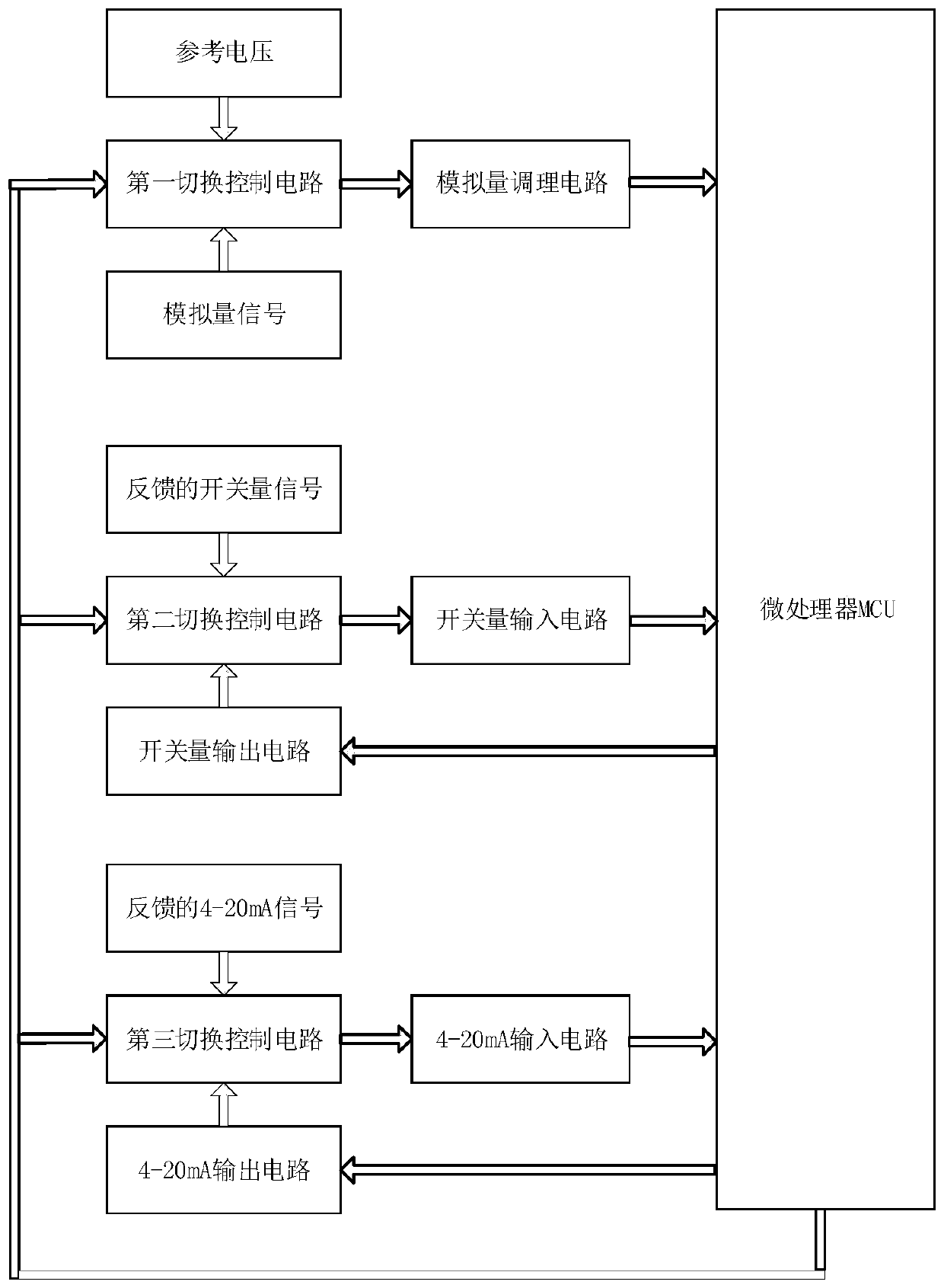
[0039] Embodiment 1: a kind of control board with testing function, see figure 1 As shown, including MCU, analog conditioning circuit, switching input circuit, switching output circuit, 4-20mA input circuit and 4-20mA output circuit, MCU is connected with analog conditioning circuit, switching input circuit, switching output circuit respectively , The 4-20mA input circuit is electrically connected with the 4-20mA output circuit, and the analog quantity conditioning circuit is used to process the input analog quantity signal, and outputs a voltage signal of 0-3V to the MCU; the control board also includes a first switching control circuit, the second switching control circuit, the third switching control circuit and the reference voltage circuit, the input terminals of the first switching control circuit, the second switching control circuit and the third switching control circuit are all connected with the control signal output terminal of the MCU, and the reference voltage Th...
Embodiment 2
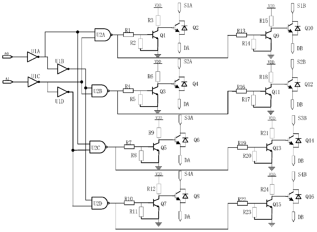
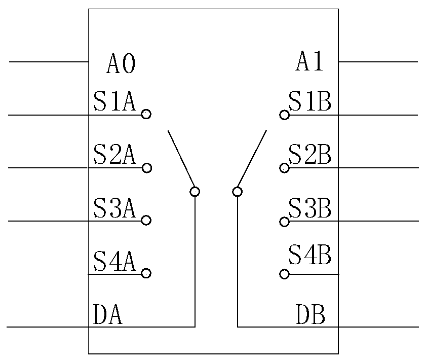
[0045] Embodiment 2: on the basis of embodiment 1, refer to figure 2 As shown, the first switching control circuit, the second switching control circuit and the third switching control circuit all include a selection signal receiving terminal A0, a selection signal receiving terminal A1, a NOT gate U1A, a NOT gate U1B, a NOT gate U1C, a NOT gate U1D, NAND gate U2A, NAND gate U2B, NAND gate U2C, the first switching channel, the second switching channel and the third switching channel, the selection signal receiving end A0 and the selection signal receiving end A1 are used to receive the channel sent by the MCU Select a signal.
[0046] The input end of the NOT gate U1A is connected to the selection signal receiving end A0, the output end of the NOT gate U1A is connected to the input end of the NOT gate U1B; the input end of the NOT gate U1C is connected to the selection signal receiving end A1, and the output end of the NOT gate U1C Connect to the input of the NOT gate U1D. ...
Embodiment 3
[0056] Embodiment 3: on the basis of embodiment 2, refer to figure 2 As shown, a voltage dividing resistor R2 is connected between the b-pole and the e-pole of the triode Q1 to stabilize the voltage difference (about 0.7V) between the b-pole and e-pole of the triode Q1, so as to ensure that the triode Q1 can reliably conduct Pass.
[0057] Based on the same principle, a voltage dividing resistor R5 is connected between the b pole and the e pole of the transistor Q3, and a voltage dividing resistor R8 is connected between the b pole and the e pole of the transistor Q5, which are used to stabilize the b poles of the transistors Q3 and Q5 respectively. The pressure difference between pole and e.
PUM
 Abstract
Description
Claims
Application Information


