
Fabrication method of asymmetric surface channel field effect transistor and power device

An asymmetric, transistor-based technology, applied in semiconductor devices, semiconductor/solid-state device manufacturing, electrical components, etc., can solve problems such as low breakdown voltage, achieve the effect of increasing breakdown voltage and operating voltage, and increasing power density

Active Publication Date: 2021-01-12
THE 13TH RES INST OF CHINA ELECTRONICS TECH GRP CORP
View PDF11 Cites 1 Cited by
  • Summary
  • Abstract
  • Description
  • Claims
  • Application Information

AI Technical Summary

Problems solved by technology

[0003] The purpose of the present invention is to provide a method for preparing an asymmetric surface channel field effect transistor, aiming to solve the technical problem of low breakdown voltage in the prior art

Method used


Image

  • Fabrication method of asymmetric surface channel field effect transistor and power device
  • Fabrication method of asymmetric surface channel field effect transistor and power device
  • Fabrication method of asymmetric surface channel field effect transistor and power device

Examples


Embodiment Construction

[0044] In order to make the technical problems, technical solutions and beneficial effects to be solved by the present invention clearer, the present invention will be further described in detail below in conjunction with the accompanying drawings and embodiments. It should be understood that the specific embodiments described here are only used to explain the present invention, not to limit the present invention.

[0045] Please also refer to Figure 1 to Figure 5 , the preparation method of the asymmetric surface channel field effect transistor provided by the present invention will now be described. The preparation method of the asymmetric surface channel field effect transistor comprises the following steps:

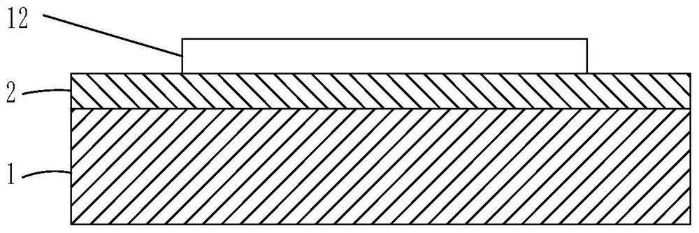
[0046] A metal mask layer 2 is deposited on the surface channel epitaxial layer 1, see figure 1 ;

[0047] Prepare the first photoresist layer 12 on the metal mask layer 2, see figure 2 ;

[0048] Exposure, development, forming source region graphics and drain ...


PUM


Abstract

The present application provides a method for fabricating an asymmetric surface-channel field-effect transistor and power device, belonging to the technical field of microwave power devices, comprising the following steps: depositing a metal mask layer; preparing a first photoresist layer; forming a source region pattern and a drain region pattern; depositing a source metal layer and a drain metal layer at the source region pattern and the drain region pattern; lifting off and removing the first photoresist; applying two photoresist layers; photolithographically etching a gate-etching window pattern and a field plate metal window pattern, and etching the metal mask layer at the corresponding location; depositing a gate metal layer and a field plate metal layer, the distance between the two sides of the gate metal layer and the corresponding unetched metal mask layer being different; the effective gate–source spacing of the device is smaller than the effective gate–drain spacing. The method for fabricating the asymmetric surface-channel field-effect transistor, and device having an effective gate–source spacing which is smaller than the effective gate–drain spacing, provided by the present application, are capable of taking into account the saturation current and effectively improving breakdown voltage and operating voltage to increase the power density of the device.

Description

technical field [0001] The invention belongs to the technical field of microwave power devices, and more specifically relates to a preparation method of an asymmetric surface channel field effect transistor and a power device. Background technique [0002] Because surface channel devices have great advantages in high speed and high confinement, they have attracted much attention in the high frequency field. Currently commonly used surface channel materials include p-type surface channels formed by hydrogen plasma treatment of diamond, and two-dimensional materials such as graphene, BN, black phosphorus, and two-dimensional GaN. The characteristics of surface channel devices are greatly affected by the surface state. The self-alignment process developed in recent years has effectively solved the above problems. However, the self-alignment process can only achieve a device structure with equal spacing between gate-source and gate-drain. In order to take into account the satur...

Claims


Application Information

Patent Timeline
IPC IPC(8): H01L21/28H01L21/44H01L21/34H01L21/336H01L29/417H01L29/423H01L29/78
CPCH01L21/28H01L21/34H01L21/44H01L29/417H01L29/423H01L29/78
Inventor 吕元杰王元刚冯志红蔚翠周闯杰宋旭波何泽召梁士雄
Owner THE 13TH RES INST OF CHINA ELECTRONICS TECH GRP CORP
Learn More