Photovoltaic battery chip and fabrication method thereof

A technology for photovoltaic cells and manufacturing methods, applied in the field of photovoltaic solar energy, capable of solving problems such as low photoelectric conversion efficiency, changes in battery chip characteristics, and affecting the service life of photovoltaic cell chips, achieving the effects of improving photoelectric conversion efficiency and improving anti-reflection effects

Pending Publication Date: 2019-05-21
上海祖强能源有限公司
View PDF0 Cites 2 Cited by
  • Summary
  • Abstract
  • Description
  • Claims
  • Application Information

AI Technical Summary

Problems solved by technology

[0004] The invention of the present application provides a photovoltaic cell chip and its manufacturing method to solve the problem that in the prior art, part of the film layer of the photovoltaic cell chip is directly exposed to the air, which causes the characteristics of the cell chip to change, which seriously affects the service life of the photovoltaic cell chip and the photoelectric conversion. inefficiency

Method used


Image

  • Photovoltaic battery chip and fabrication method thereof
  • Photovoltaic battery chip and fabrication method thereof

Examples


Embodiment Construction

[0030] In the following description, numerous specific details are set forth in order to provide a thorough understanding of the application. However, the present application can be implemented in many other ways different from those described here, and those skilled in the art can make similar promotions without violating the connotation of the present application. Therefore, the present application is not limited by the specific implementation disclosed below.

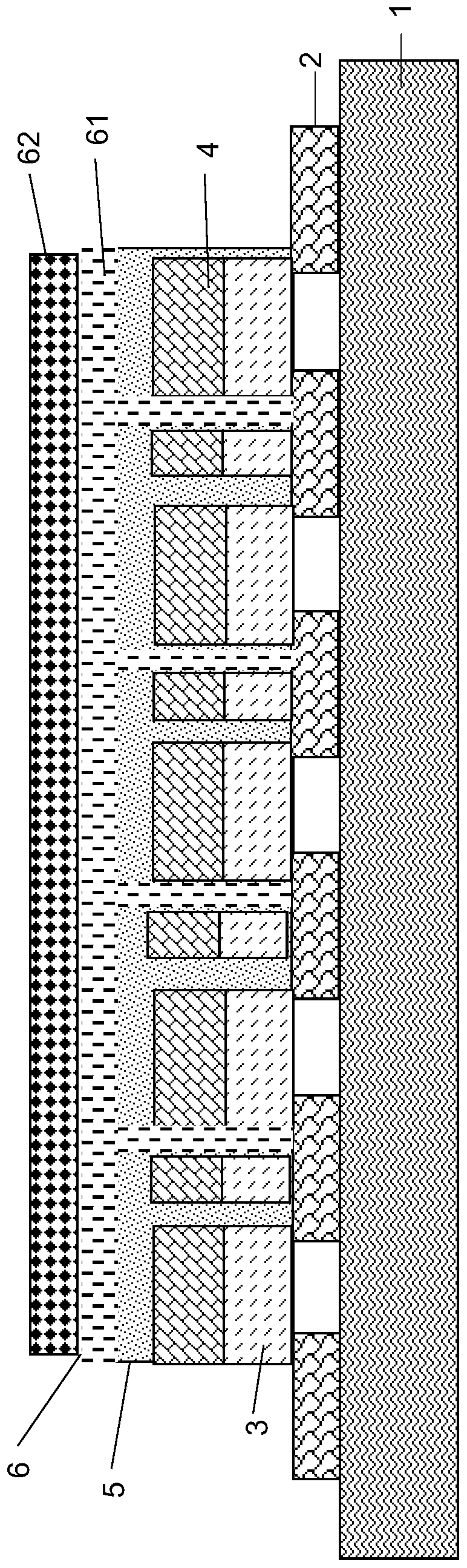
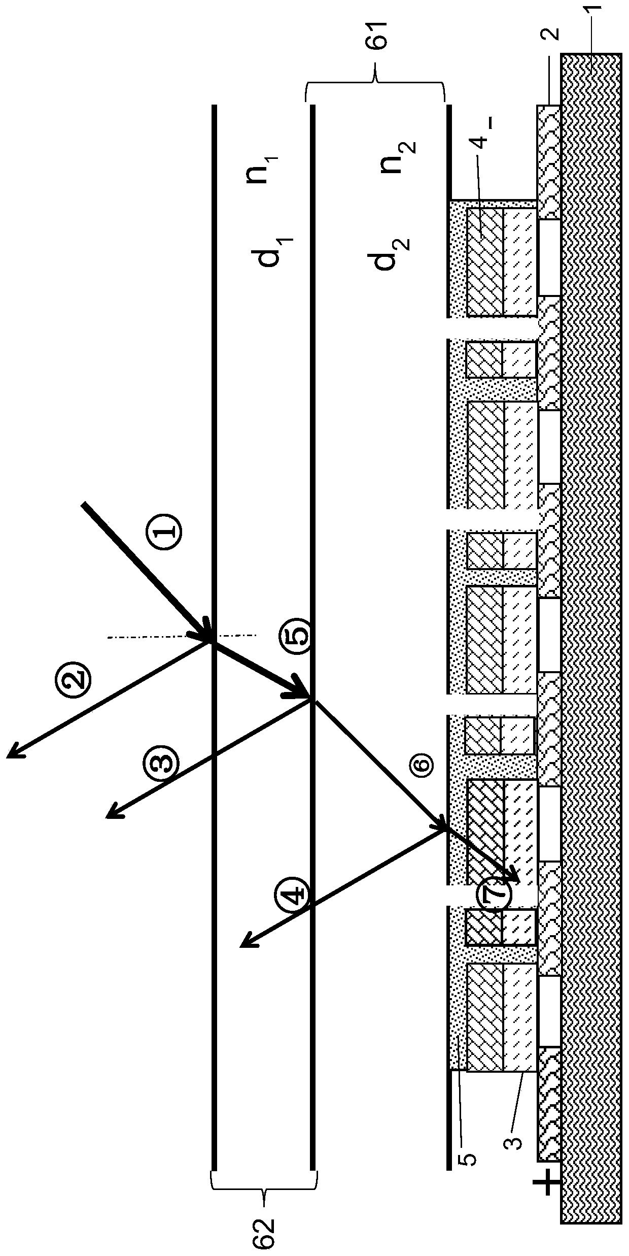
[0031] see figure 1 A photovoltaic cell chip provided by an embodiment of the present invention includes a substrate 1, a first electrode layer 2, a semiconductor layer (P-type semiconductor layer 3, and an N-type semiconductor layer 4), a light-transmitting second electrode layer 5, And at least one anti-reflection film combination layer 6. Wherein, according to the direction from close to the substrate 1 to away from the substrate 1, the first electrode layer 2, the P-type semiconductor layer 3, the N-type semicon...


PUM


Abstract

The invention discloses a photovoltaic battery chip and a fabrication method thereof. The photovoltaic battery chip comprises a matrix, a semiconductor layer, a first electrode layer and a second transmitting electrode layer, wherein the first electrode layer and the second electrode layer are arranged at two opposite layers of the semiconductor layer, at least one anti-reflection film combinationlayer is attached onto a surface, far away from the semiconductor layer, of the second electrode layer, the anti-reflection film combination layer comprises a first anti-reflection film layer and a second anti-reflection film layer, the first anti-reflection film layer is formed on a surface of the second electrode layer, the second anti-reflection film layer is formed on a surface of the first anti-reflection film layer, the refractivity of the first anti-reflection layer is smaller than the refractivity of the second anti-reflection film layer, and the refractivity of the first anti-reflection layer is smaller than the refractivity of the second electrode layer. The surface of the second electrode layer can be covered and protected very well by the anti-reflection film layer combinationlayer contained in the photovoltaic battery chip provided by the invention, the anti-reflection effect is effectively improved, the photoelectric conversion efficiency of the photovoltaic battery chip is greatly improved, and the service lifetime of the photovoltaic battery chip is prolonged.

Description

technical field [0001] The application of the present invention relates to the technical field of photovoltaic solar energy, in particular to a photovoltaic cell chip and a manufacturing method thereof. Background technique [0002] Currently existing solar cells mainly include silicon-based solar cells and thin-film solar cells. A solar cell refers to a device that receives solar radiation, absorbs solar energy, and converts solar energy directly into electrical energy, including multiple PN junctions formed by P-type semiconductor materials and N-type semiconductor materials. Under the irradiation of light, there will be a concentration difference between electrons and holes at the interface of the PN junction. The holes in the N-type semiconductor move to the P region, and the electrons in the P region move to the N region, thus forming a transition from the N region to the P region. The current in the region, and then a potential difference is formed in the PN junction....

Claims


Application Information

Patent Timeline
Patent Type & Authority Applications(China)
IPC IPC(8): H01L31/0216H01L31/18
CPCY02P70/50
Inventor 黄亮谭军毅任星星吴根辉段文芳
Owner 上海祖强能源有限公司
Why Eureka
Try Eureka