A compact x-shaped artificial surface plasmon waveguide

A plasma and artificial surface technology, applied in the directions of waveguides, waveguide-type devices, circuits, etc., can solve the problems of reducing the size of the waveguide structural unit and increasing the waveguide bandwidth to transmit surface waves.

Active Publication Date: 2021-07-06
UNIV OF ELECTRONICS SCI & TECH OF CHINA
View PDF4 Cites 0 Cited by
  • Summary
  • Abstract
  • Description
  • Claims
  • Application Information

AI Technical Summary

Problems solved by technology

Scholars have proposed many different forms of sub-wavelength structures to realize electromagnetic wave transmission in the microwave band, but there are still many challenges in reducing the size of the waveguide structural unit, increasing the bandwidth of the waveguide, and the ability of the waveguide to bind the transmitted surface waves.

Method used


Image

  • A compact x-shaped artificial surface plasmon waveguide
  • A compact x-shaped artificial surface plasmon waveguide
  • A compact x-shaped artificial surface plasmon waveguide

Examples


Embodiment Construction

[0028] The present invention will be further described below in conjunction with the accompanying drawings and embodiments.

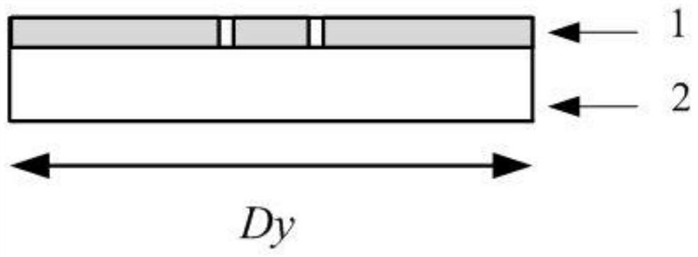
[0029] This embodiment provides a compact X-shaped artificial surface plasmon waveguide, its left view and top view are as follows figure 1 and figure 2 As shown, it is axisymmetrically distributed, including metal copper clad layer 1 and dielectric layer 2; the thickness of the metal copper clad layer is 0.035mm, the relative dielectric constant of the dielectric layer is equal to 2.67, and the thickness is 0.5mm, D y =41.52mm.

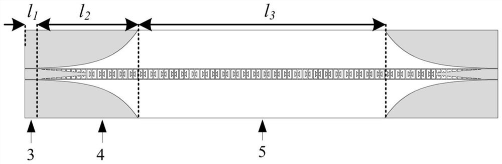
[0030] From left to right, the metal copper cladding is the first coplanar waveguide 3, the first transition structure 4, the X-shaped SSPPs structure 5 arranged periodically, the second transition structure and the second coplanar waveguide, where l 1 = 5mm, l 2 =50mm, l 3 =120mm.

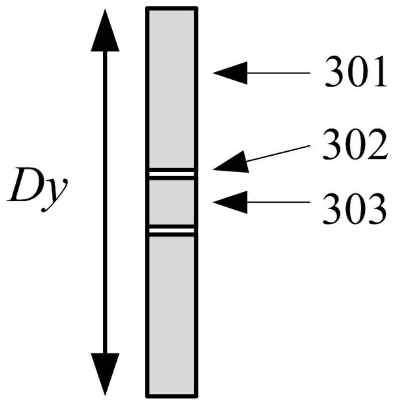
[0031] The coplanar waveguide is a 50Ω coplanar waveguide, and its structure diagram is as follows image 3 As shown, from top to bottom a...


PUM

PropertyMeasurementUnit
thicknessaaaaaaaaaa
thicknessaaaaaaaaaa
widthaaaaaaaaaa

Abstract

The invention discloses an X-shaped artificial surface plasma waveguide with a compact structure, belongs to the technical field of artificial surface plasma and waveguide, and is suitable for artificial surface plasma devices or circuits in the microwave frequency band. The present invention includes a metal copper cladding layer and a dielectric layer; the metal copper cladding layer is sequentially from left to right a first coplanar waveguide, a first transition structure, a periodically arranged X-shaped SSPPs structure, a second transition structure and a second coplanar waveguide . The present invention uses coplanar waveguide excitation, and combines the coplanar waveguide and X-shaped SSPPs structure through a transition structure to obtain an X-shaped single-conductor waveguide based on an artificial surface plasmon structure. The simulation results show that in the working frequency band of 2.5-12.6GHz, the The reflection coefficient at the input end of the structure is lower than -10dB, the transmission coefficient at the output end is greater than -3dB, and the group delay in the entire working frequency band is lower than 2.6ns.

Description

technical field [0001] The invention belongs to the technical field of artificial surface plasma and waveguide, in particular to an X-shaped artificial surface plasma waveguide with a compact structure, which is suitable for artificial surface plasma devices or circuits in the microwave frequency band. Background technique [0002] For a long time, people have been committed to studying the propagation process of electromagnetic waves, and constraining and regulating electromagnetic waves by designing a series of components that can meet different needs. Research in recent years has shown that artificial surface plasmons can be connected with knowledge in the fields of terahertz technology, microwave technology, metamaterials, and photonic crystals, and have broad application prospects, such as highly integrated optical circuits, super-resolution imaging and data storage etc. The new generation of communication technology requires smaller size and spatial layout of componen...

Claims


Application Information

Patent Timeline
Patent Type & Authority Patents(China)
IPC IPC(8): H01P3/00
Inventor 王晓华万晔聂荣邹
Owner UNIV OF ELECTRONICS SCI & TECH OF CHINA
Why Eureka
Try Eureka