
Packaging shielding structure and electronic equipment

A technology of shielding structure and shielding layer, applied in the fields of magnetic field/electric field shielding, circuits, printed circuits, etc., can solve the problems of unsatisfactory grounding effect of system-level packaging and poor electromagnetic shielding effect.

Active Publication Date: 2019-05-24
HUAWEI TECH CO LTD
View PDF5 Cites 8 Cited by
  • Summary
  • Abstract
  • Description
  • Claims
  • Application Information

AI Technical Summary

Problems solved by technology

The grounding method and structure of the SIP shielding are very important. It is necessary to ensure that the grounding of the shielding layer and the substrate forms a good Faraday cage to form a good electromagnetic shielding. However, the grounding effect of the system-in-package in the prior art is not ideal, resulting in electromagnetic shielding less effective

Method used


Image

  • Packaging shielding structure and electronic equipment
  • Packaging shielding structure and electronic equipment
  • Packaging shielding structure and electronic equipment

Examples


Embodiment Construction

[0042] In order to make the purpose, technical solution and advantages of the application clearer, the application will be further described in detail below in conjunction with the accompanying drawings.

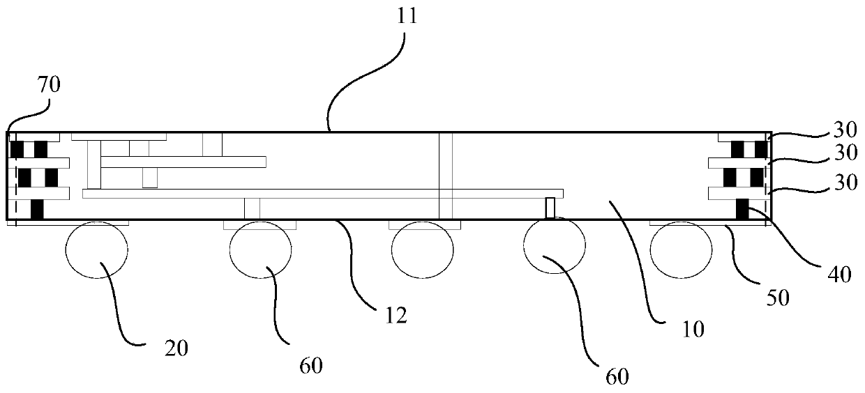
[0043] In order to facilitate the understanding of the encapsulation and shielding structure provided by the embodiment of the present application, firstly, its application scenario is explained. The encapsulation and shielding structure can be applied to SIP or non- In SIP encapsulation. Such as power modules in mobile phones, radio frequency modules, etc. When in use, it is necessary to set up the device on the circuit board, and then package the device through the shielding layer. When realizing shielding, the shielding layer needs to be grounded. When the package shielding structure is used, it may be on the side wall of the circuit board or the circuit Signal interference exists on the surface of the board. In order to improve the shielding effect of the shielding laye...


PUM

PropertyMeasurementUnit
Diameteraaaaaaaaaa
Diameteraaaaaaaaaa

Abstract

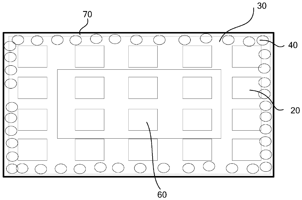
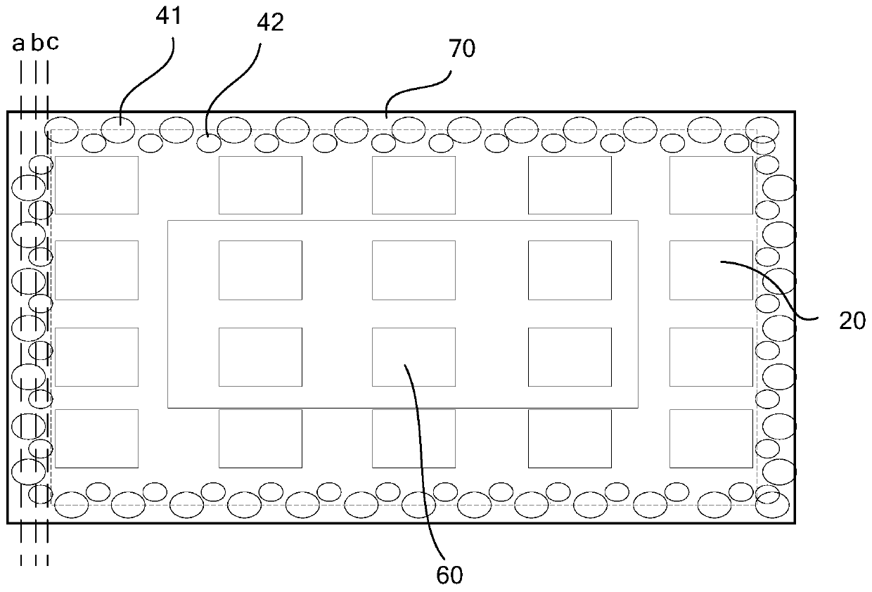
The invention provides a shielding packaging structure and electronic equipment, and the shielding packaging structure comprises a substrate. At least two stacked first grounding layers are arranged in the substrate, and one surface of the substrate is provided with a second grounding layer. The second grounding layer is provided with grounding bonding pads arranged along the edge of the substrate. Moreover, grounding holes for electrically connecting the adjacent grounding layers are formed in the substrate, and the grounding holes are arranged in a circle around a plate body, and the distance between the adjacent grounding holes is smaller than a set distance, so that the grounding holes can form a good Faraday electric cage. A device is arranged on the other surface of the substrate, and a packaging layer for packaging the device is also arranged on the device. In addition, the structure also comprises a shielding layer wrapped by the packaging layer, and the shielding layer extendsto the substrate and is electrically connected with the first grounding layers. According to the scheme, the grounding resistance is reduced through the arranged grounding holes, and the electromagnetic shielding effect of the shielding layer is improved. Electromagnetic interference at the bottom of the substrate is avoided through the second grounding layer and the grounding bonding pad, and the shielding effect is improved.

Description

technical field [0001] The present application relates to the technical field of mobile terminals, in particular to a packaging and shielding structure and electronic equipment. Background technique [0002] With the development of SiP (System-in-Package, system-in-package) technology and the demand for miniaturization of mobile phones, packaging technology is used to integrate active modules and passive devices into a system at the packaging level to increase device integration. , thereby reducing the device area on the PCB and improving the integration and simplicity of the PCB. Using a large number of SiPs to make customized modules is also an important way for the current miniaturization of mobile phones. The grounding method and structure of the SIP shielding are very important. It is necessary to ensure that the grounding of the shielding layer and the substrate forms a good Faraday cage to form a good electromagnetic shielding. However, the grounding effect of the sy...

Claims


Application Information

Patent Timeline
IPC IPC(8): H05K9/00
CPCH01L2924/3025H01L2924/15311H01L2924/15192H01L23/552H01L23/3128H01L23/49822H01L21/561H01L23/562H01L23/585H01L23/49816H05K1/0224H05K2201/0723
Inventor 王惠娟蔡锦森胡彬孔博肇天
Owner HUAWEI TECH CO LTD
Learn More