Electromagnetic pulse welding system special for PCB welding

An electromagnetic pulse, PCB board technology, used in welding equipment, electric heating devices, printed circuits, etc., can solve problems such as soldering off, device performance degradation, and increased contact resistance, to ensure cleanliness and reduce welding steps.

Active Publication Date: 2019-05-28
CHONGQING UNIVERSITY OF SCIENCE AND TECHNOLOGY
View PDF7 Cites 6 Cited by
  • Summary
  • Abstract
  • Description
  • Claims
  • Application Information

AI Technical Summary

Problems solved by technology

There are many welding steps, so it is necessary to ensure that each step is qualified for product quality. At the same time, there are multiple solder joints and multiple electronic components on the printed circuit board, so multiple soldering is required
At the same time, soldering is used, because flux, solder, etc. will be introduced, so it is easy to cause the surface of the chip to be unclean, and additional cleaning steps are often required
[0004] Furthermore, the failure of electronic equipment is often caused by various problems in the soldering process, such as: the pressure welding is too heavy, causing the welding place to break; the pressure welding is too light or the surface of the chip is not clean, resulting in false welding Falling off; intermetallic compounds, such as Au-Al, may form Au at the soldering place 2 Al, AuAl, AuAl 2 、Au 4 Al, Au 5 Al, etc., have different lattice constants and expansion coefficients, and lower conductivity, resulting in reduced bonding strength and increased contact resistance, leading to device performance degradation or failure.

Method used


Image

  • Electromagnetic pulse welding system special for PCB welding
  • Electromagnetic pulse welding system special for PCB welding
  • Electromagnetic pulse welding system special for PCB welding

Examples


Embodiment 1

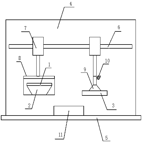
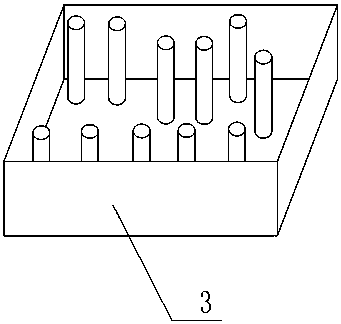
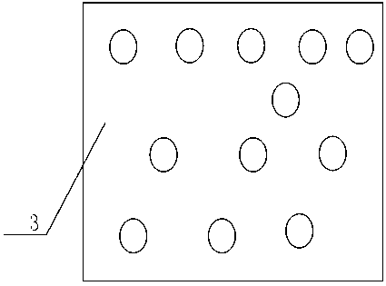
[0024] An electromagnetic pulse welding system specially used for PCB board welding, including a bearing base 5, an electromagnetic pulse welding assembly, and a shielding mold 3. This embodiment defines the PCB board to be welded, that is, the back side of the printed circuit board 12 is provided with a number of solder joints 14 arranged in an array and holes passing through the electronic components, and the electronic components pass through the holes, and the pins of the electronic components 13 is bent to correspond to the solder joint 14 on the back of the printed circuit board 12 , and has a certain distance from the solder joint 14 . Such a PCB board to be soldered is placed on the carrying base 5 with its back facing upwards.

[0025] The electromagnetic pulse welding assembly includes a pulse power supply, a coil 1 and a flat magnet collector 2, and the coil 1 is located above the flat magnet collector 2 and connected to the pulse power supply.

[0026] Specificall...

Embodiment 2

[0031] The difference between this embodiment and Embodiment 1 is that a limiting frame or a limiting seat 11 is provided on the bearing base 5, and the boundary of the PCB board can be placed on the limiting frame for support.

[0032] The limit seat 11 is a boss and is provided with a plurality of placement grooves matching the size and position of the electronic components on the PCB board to be soldered.

Embodiment 3

[0034] The difference between this embodiment and Embodiment 1 is that other designs are made to improve the mechanization of the system.

[0035] In this embodiment, the mounting frame 8 is made of non-conductive material, and the mounting frame 8 is an inverted L-shaped structure, and the coil 1 and the flat magnetic collector 2 are bonded to the mounting frame 8 by an adhesive. The supporting base 5 is provided with a support plate 4, and the top of the installation frame 8 is set on the support plate 4 through the electric push rod 7, so that the flat magnetic collector 2 can move up and down, which is convenient for placing and taking out the PCB board.

[0036] Further, the electric push rod 7 is connected with the support plate 4 through the slider, and the support plate 4 is provided with a horizontally arranged electric slide rail 6 for the slider to slide, so that the electromagnetic pulse assembly can move left and right and up and down on the support plate 4 .

[...


PUM


Abstract

The invention discloses an electromagnetic pulse welding system special for PCB welding. The electromagnetic pulse welding system special for PCB welding comprises a bearing base used for containing ato-be-welded PCB, an electromagnetic pulse welding assembly and a shield mold. The electromagnetic pulse welding assembly comprises a pulse power source, a coil and a plate magnetic collector, and the coil is located above the plate magnetic collector and connected with the pulse power source. The electromagnetic pulse welding assembly is arranged above the bearing base through an installation frame on the bearing base; and the shield mold is used for covering the back face of the PCB and made of a non-conductor material, the whole shield mold is a box cover capable of covering a bottom opening of the PCB, multiple non-shield channels vertically penetrating through the box cover are arranged in the box cover, and the non-shield channels correspond to welding points of the back face of theto-be-welded PCB one to one.

Description

technical field [0001] The invention relates to the technical field of electromagnetic pulse welding, in particular to a system for welding PCB boards by using the electromagnetic pulse welding technology. Background technique [0002] The production process of PCB is to design the drawing first, then print the drawing design on the printed circuit board to form pads with solder joints and formed circuits, and then install the electronic components on the pads and connect them to the pads. In an existing welding method, spherical pads are arranged in a two-dimensional array on the back of the printed circuit substrate, and holes for component insertion are opened on the printed circuit substrate. After the components are inserted into the holes, the solder joints between the pins and the basic back of the printed circuit Soldering, such as the grid array package is used in this way. [0003] However, no matter what kind of package soldering technology is used, the connectio...

Claims


Application Information

Patent Timeline
Patent Type & Authority Applications(China)
IPC IPC(8): B23K3/047B23K1/005B23K101/42
Inventor 王刚曹磊磊张中文许章亮张丽萍
Owner CHONGQING UNIVERSITY OF SCIENCE AND TECHNOLOGY
Why Eureka
Try Eureka