High-voltage LED chip structure and manufacturing method thereof

An LED chip and manufacturing method technology, applied in electrical components, electric solid state devices, circuits, etc., can solve the problems of small light-emitting area and low light-emitting efficiency of the chip, reduce the area, increase the area of ​​the light-emitting area, and improve the light emitting area. effective effect

Active Publication Date: 2019-05-28
XIAMEN CHANGELIGHT CO LTD
View PDF5 Cites 9 Cited by
  • Summary
  • Abstract
  • Description
  • Claims
  • Application Information

AI Technical Summary

Problems solved by technology

[0006] In view of this, the present invention provides a high-voltage LED chip structure and its manufacturing method to solve the problem of low luminous efficiency of the entire chip caused by the existence of the original cell isolation area of ​​the high-voltage LED chip in the prior art, which leads to the reduction of the area of ​​the light-emitting area. question

Method used


Image

  • High-voltage LED chip structure and manufacturing method thereof
  • High-voltage LED chip structure and manufacturing method thereof
  • High-voltage LED chip structure and manufacturing method thereof

Examples


Embodiment Construction

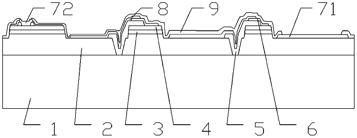
[0049] As mentioned in the background art, the luminous efficiency of the high-voltage LED chips in the prior art is relatively low.

[0050] The inventor found that the root cause of the above-mentioned problems in the prior art is that the high-voltage LED chip includes a primary cell isolation area, which occupies the area of ​​the light-emitting area, making the area of ​​the light-emitting area smaller, thereby affecting the luminous efficiency of the entire chip .

[0051] Based on this, the present invention provides a high-voltage LED chip structure, including:

[0052] Multiple LED chip particles;

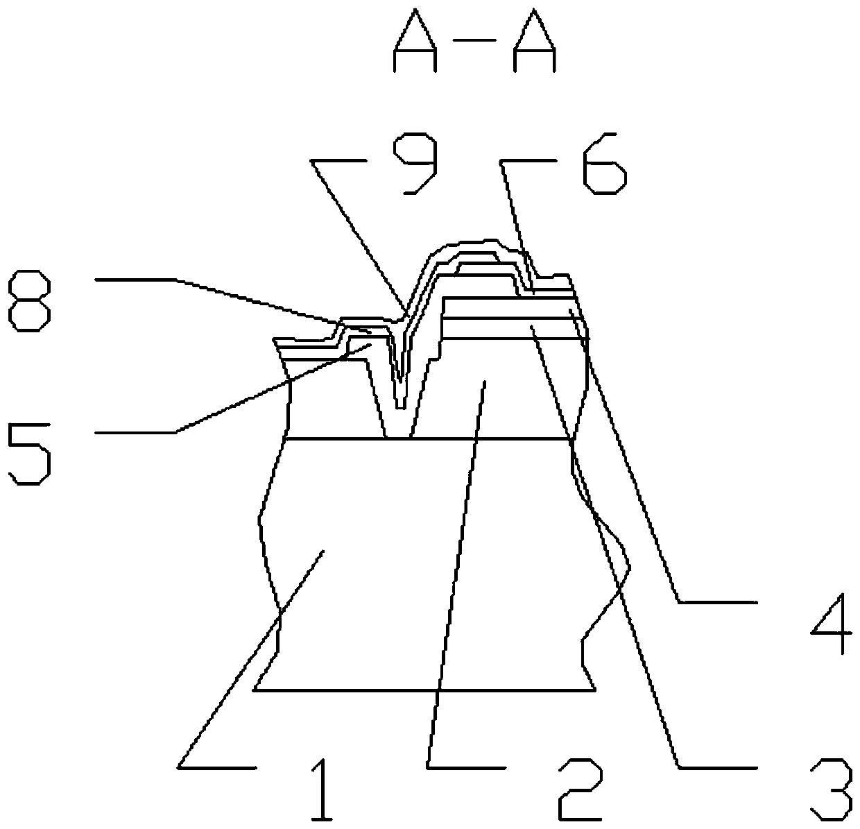
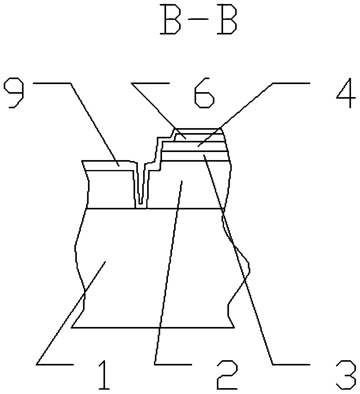
[0053] A cell isolation groove is arranged between two adjacent LED chip particles;

[0054] The cell isolation groove includes a connection area cell isolation groove for connecting two adjacent LED chip particles and a non-connection area cell isolation groove located outside the connection area cell isolation groove;

[0055] In the direction of the connecting line bet...


PUM


Abstract

The invention provides a high-voltage LED chip structure and a manufacturing method thereof. The high-voltage LED chip structure comprises a plurality of LED chip particles and primitive cell isolation grooves formed between every two adjacent LED chip particles, wherein each primitive cell isolation groove comprises a connecting area primitive cell isolation groove and a non-connecting area primitive cell isolation groove, and the width of the non-connecting area primitive cell isolation groove is smaller than that of the connecting area primitive cell isolation groove in the direction of a connecting line of centers of two adjacent LED chip particles; and the inclination of the side wall of the non-connection area primitive cell isolation groove is greater than that of the side wall of the connection area primitive cell isolation groove. Therefore, the area of the non-connecting area primitive cell isolation groove is reduced, the area of the light-emitting area is increased, and thelighting effect of the high-voltage LED chip is improved. Due to the fact that the side wall of the connection area primitive cell isolation groove is slow, effective coverage of a bridge connectioninsulation isolation layer and a bridge connection electrode is guaranteed, and the product reliability of the high-voltage LED chip structure is guaranteed.

Description

technical field [0001] The invention relates to the technical field of manufacturing semiconductor devices, in particular to a high-voltage LED chip structure and a manufacturing method thereof. Background technique [0002] The light-emitting principle of light-emitting diodes (LEDs) is to use the energy difference between electrons moving between n-type semiconductors and p-type semiconductors to release energy in the form of light. This light-emitting principle is different from that of incandescent lamps, so light-emitting diodes are used called a cold light source. In addition, light-emitting diodes have the advantages of high durability, long life, light weight, and low power consumption. Therefore, today's lighting market places high hopes on light-emitting diodes and regards them as a new generation of lighting tools. [0003] However, the current LED chip still has the problem of low luminous efficiency. Therefore, improving the luminous efficiency of light-emitti...

Claims


Application Information

Patent Timeline
Patent Type & Authority Applications(China)
IPC IPC(8): H01L33/20H01L33/00H01L27/15
Inventor 刘英策李俊贤刘兆魏振东黄瑄
Owner XIAMEN CHANGELIGHT CO LTD
Why Eureka
Try Eureka