Organic electroluminescent device

An electroluminescent device and luminescent technology, applied in the direction of organic semiconductor devices, electric solid devices, electrical components, etc., can solve the problems of low efficiency of light-emitting devices, achieve low roll-off, improve luminous efficiency, and high efficiency

Inactive Publication Date: 2019-05-28
KUNSHAN GO VISIONOX OPTO ELECTRONICS CO LTD +1
View PDF3 Cites 17 Cited by
  • Summary
  • Abstract
  • Description
  • Claims
  • Application Information

AI Technical Summary

Problems solved by technology

[0006] Therefore, the present invention is to solve the problem of low efficiency of fluorescent electroluminescent devices in the prior art

Method used


Image

  • Organic electroluminescent device
  • Organic electroluminescent device
  • Organic electroluminescent device

Examples


Embodiment 1

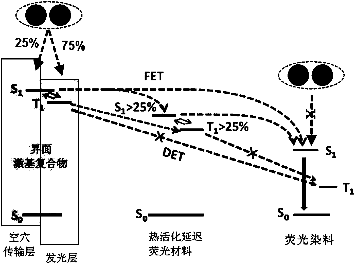
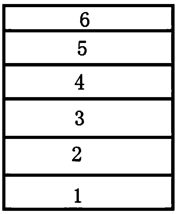
[0042] This embodiment provides an organic electroluminescent device, such as figure 2 As shown, it includes a first electrode 1, a hole transport layer 2, a light emitting layer 3, an electron transport layer 4, an electron injection layer 5 and a second electrode. As an embodiment of the present invention, specifically, the structure of the organic electroluminescent device is: ITO / TAPC (50nm) / TCTA (10nm) / light-emitting layer (30nm) / BPBiPA (30nm) / LiF (0.5nm) / Al (150nm). Wherein, the light-emitting layer 3 includes the first host material PhCzTRz, the TADF sensitizer PXZ-DPS, and the fluorescent dye PhtBuPAD. The specific structure is as follows:

[0043]

[0044] Among them, triplet energy level: TCTA is greater than PhCzTrz and PhtBuPAD.

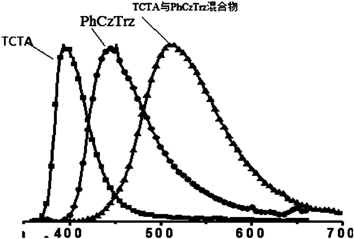
[0045] Such as image 3 The hole transport layer material and the first host material mixture (TCTA and PhCzTrz mixture) spectra are obviously red-shifted compared to the hole transport layer material (TCTA) and the first host material (PhC...

Embodiment 2

[0047] This embodiment provides an organic electroluminescent device, the structure of which is the same as that of Embodiment 1, and the first host material is replaced with:

[0048]

Embodiment 3

[0050] This embodiment provides an organic electroluminescent device, the structure of which is the same as that of embodiment 1, and the TADF material is replaced with:

[0051]


PUM


Abstract

The invention belongs to the technical field of display, and particularly relates to an organic electroluminescent device, in particular to an efficient fluorescent device. The organic electroluminescent device includes a thermally activated delayed fluorescent material, a first host material, and a fluorescent dye. A hole transport layer can form an interfacial exciplex with the first host material and further sensitize the fluorescent dye by using the thermally activated delayed fluorescent material as a sensitizer. According to the thermal activation delayed fluorescence (TSF) organic electroluminescent device prepared by the method, the external quantum efficiency exceeds the external quantum efficiency of a traditional fluorescent device by about 5%, the luminous efficiency of a fluorescent OLED device is greatly improved, and meanwhile, theorganic electroluminescent device has the advantages of low turn-on voltage, low roll-off and the like.

Description

Technical field [0001] The invention belongs to the field of display technology, and specifically relates to an organic electroluminescence element. Background technique [0002] Organic light-emitting diodes (OLEDs) have great application prospects in the display and lighting fields due to their advantages such as ultra-thin, light weight, low energy consumption, active light emission, wide viewing angle, and fast response. People pay more attention. [0003] In 1987, Deng Qingyun (CWTang) and Vanslyke of Eastman Kodak Company in the United States reported for the first time the use of a transparent conductive film as the anode, Alq3 as the light-emitting layer, triarylamine as the hole transport layer, and Mg / Ag alloy as the cathode. Layer organic electroluminescent device. Traditional fluorescent materials are easy to synthesize, the materials are stable, and the device life is long. However, due to the electron spin forbidden, only 25% of singlet excitons can be used to emit ...

Claims


Application Information

Patent Timeline
Patent Type & Authority Applications(China)
IPC IPC(8): H01L51/54H01L51/50
CPCH10K85/623H10K85/615H10K85/656H10K85/654H10K50/121H10K85/633H10K85/657H10K85/6572H10K50/11H10K2101/40H10K50/15H10K2101/20H10K85/30H10K85/381H10K85/622H10K85/624H10K85/631H10K85/636H10K85/6565H10K2101/30
Inventor 段炼张东东宋晓增蔡明瀚魏金贝
Owner KUNSHAN GO VISIONOX OPTO ELECTRONICS CO LTD
Why Eureka
Try Eureka