Sensor chip based on waveguide coupling surface plasmon resonance
A surface plasmon and sensor chip technology, applied in the field of ion sensing, can solve the problems that limit the practical application of long-range SPPs detection
- Summary
- Abstract
- Description
- Claims
- Application Information
AI Technical Summary
Problems solved by technology
Method used
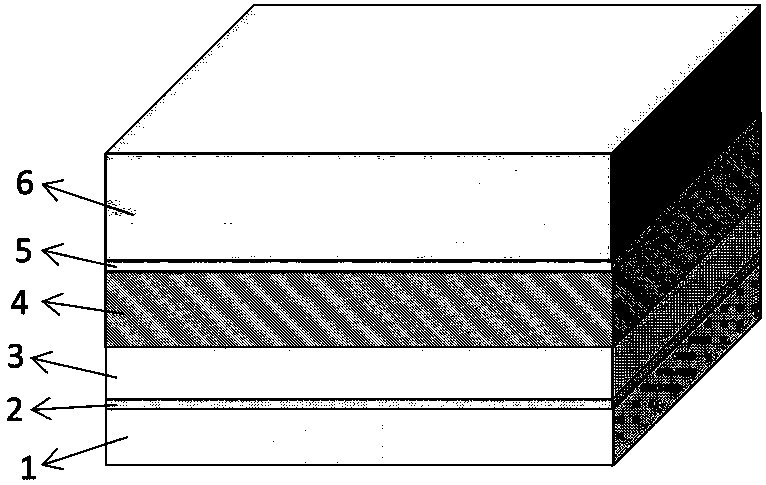
Image

Examples
Embodiment 1
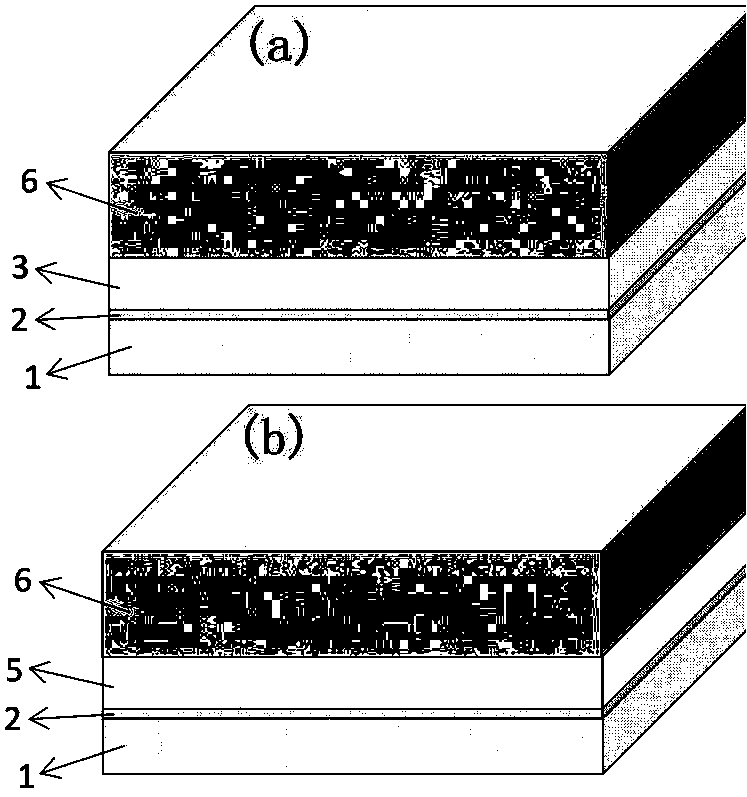
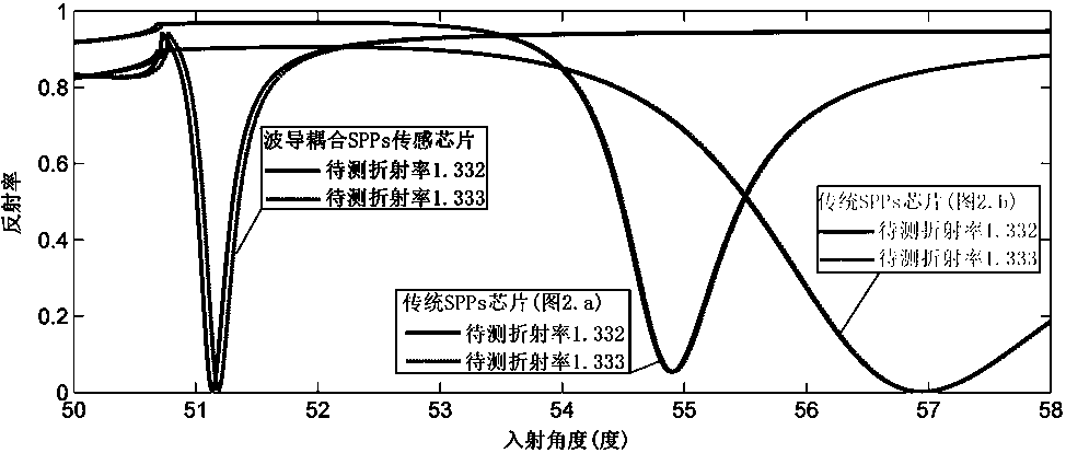
[0019] This example will combine figure 2 and image 3 Demonstrate the improvement of the detection performance of the waveguide coupling SPPs sensor chip proposed in the present invention.
[0020] In order to compare with the traditional SPPs sensor chip, figure 2 A schematic diagram of the traditional SPPs sensor chip structure is given: figure 2 (a) The thickness of the metal thin film layer 3 in the chip shown in (a) is 40 nanometers, and the material is silver; figure 2 The thickness of the metal thin film layer 5 in the chip shown in (b) is 40 nanometers, and the material is gold.
[0021] image 3 The reflectivity of the waveguide-coupled SPPs sensor chip and the traditional SPPs sensor chip are described. The solid line and the dotted line represent the reflectivity before and after the change of 0.001 in the refractive index of the sample to be tested. The angular sensitivity is defined as the change rate of the SPPs resonance angle compared with the measured...
Embodiment 2
[0023] This example will combine Figure 4 Demonstrate the adjustability of the evanescent field depth of SPPs.
[0024] Figure 4 The mode field strength distribution of waveguide-coupled SPPs is described: Figure 4 (a) The refractive index of the dielectric waveguide layer material is set to 2.198, Figure 4 (b) The refractive index of the dielectric waveguide layer material is set to 2.298. Depend on Figure 4 It can be clearly seen that as the refractive index of the material of the dielectric waveguide layer increases, the depth of the evanescent field of the waveguide-coupled SPPs mode becomes smaller. For example, when the refractive index of the material of the dielectric waveguide layer increases by 0.1, the depth of the evanescent field of the waveguide-coupled SPPs mode decreases half. The variable refractive index of the dielectric waveguide layer can be realized by thermo-optic or electro-optic effects. Therefore, this embodiment fully demonstrates that the ...
PUM
| Property | Measurement | Unit |
|---|---|---|
| Thickness | aaaaa | aaaaa |
| Thickness | aaaaa | aaaaa |
| Thickness | aaaaa | aaaaa |
Abstract
Description
Claims
Application Information
 - R&D
- Intellectual Property
- Life Sciences
- Materials
- Tech Scout
- Unparalleled Data Quality
- Higher Quality Content
- 60% Fewer Hallucinations
Browse by: Latest US Patents, China's latest patents, Technical Efficacy Thesaurus, Application Domain, Technology Topic, Popular Technical Reports.
© 2025 PatSnap. All rights reserved.Legal|Privacy policy|Modern Slavery Act Transparency Statement|Sitemap|About US| Contact US: help@patsnap.com