Two-stage three-phase soft-switching current transformer

A soft switching and converter technology, applied in the direction of converting DC power input to DC power output, AC power input converting to DC power output, instruments, etc. It can achieve the effect of high circuit efficiency, low switching loss, and improved power density.

Inactive Publication Date: 2019-05-31
ZHEJIANG UNIV
2 Cites 3 Cited by

AI-Extracted Technical Summary

Problems solved by technology

[0002] The traditional two-stage three-phase converter circuit includes four sets of half-bridge arms; the first half-bridge arm and the input side inductor form a DC-DC converter, the second half-bridge arm, and the third half-bridge arm The bridge arm, the fourth half-bridge arm and three AC side inductors form a three-phase DC-AC converter connected to the three-phase grid; the upper and lower ends of the four bridge arms are connected in parallel to form positive and negative busbars directly connected to the DC The bus capacitor...

Abstract

The invention discloses a two-stage three-phase soft-switching current transformer which comprises a front-stage DC/DC transformer and a rear-stage three-phase DC/AC transformer. A resonant branch composed of an auxiliary switching tube having an anti-parallel diode, a clamp capacitor and a resonant inductor is connected between a positive common bus of the front and rear stages and an intermediate DC-side capacitor. A resonant capacitor is connected in parallel with main switching tubes and the auxiliary switching tube. The auxiliary switching tube is synchronized with the driving pulse signals of the main switching tubes in the current transformers in the front and rear stages, so as to realize zero-voltage turning-on of all the switching tubes in each switching period, and suppress thereverse recovery current of the anti-parallel diodes of the main switching tubes. The two-stage three-phase soft-switching current transformer is low in switching loss, high in circuit efficiency, andcontributes to increasing the switching frequency and increasing the system power density.

Application Domain

Efficient power electronics conversionAc-dc conversion +2

Technology Topic

CapacitanceResonant capacitor +11

Image

  • Two-stage three-phase soft-switching current transformer
  • Two-stage three-phase soft-switching current transformer
  • Two-stage three-phase soft-switching current transformer

Examples

  • Experimental program(1)

Example Embodiment

[0013] The present invention will be described in detail below in conjunction with specific embodiments. The following examples will help those skilled in the art to further understand the present invention, but do not limit the present invention in any form. It should be noted that those skilled in the art can make several modifications and improvements without departing from the concept of the present invention. These all belong to the protection scope of the present invention. The present invention will be described in detail below in conjunction with the accompanying drawings.
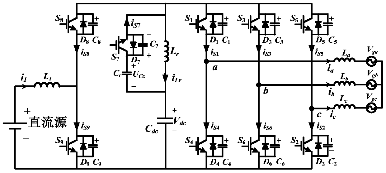
[0014] refer to figure 1 , the two-stage three-phase soft-switching converter circuit includes an AC side filter inductor L a , L b , L c; DC input side inductance L 1; Four groups of half-bridge arms; DC side capacitor C dc; and a group consisting of a parallel diode D 7 The auxiliary switch tube S 7 , Resonant inductance L r , clamp capacitor C c The auxiliary resonant branch formed by the auxiliary switching tube S 7 with clamp capacitor C c After series connection and resonant inductance L r Parallel connection; each set of half-bridge arms is composed of two series-connected fully-controlled main switch tubes containing anti-parallel diodes, and the upper and lower main switch tubes of the first bridge arm and their anti-parallel diodes are respectively S 8 , S 9 and D 8 、D 9 , the upper and lower main switching tubes and their anti-parallel diodes of the second bridge arm are respectively S 1 , S 4 and D 1 、D 4 , the upper and lower main switching tubes and their anti-parallel diodes of the third bridge arm are respectively S 3 , S 6 and D 3 、D 6 , the upper and lower main switching tubes and their anti-parallel diodes of the fourth bridge arm are respectively S 5 , S 2 and D 5 、D 2 , the upper and lower ends of the four groups of bridge arms are connected in parallel to form a positive and negative common bus; the positive common bus and the DC side capacitor C dc The above-mentioned auxiliary resonant branch is connected between them; the midpoint of the first bridge arm is connected to the inductor L 1 end of the L 1 The other end of the DC source is connected to the positive end of the input DC source, and the negative end of the DC source is connected to the negative common bus; the midpoints of the second bridge arm, the third bridge arm, and the fourth bridge arm are respectively connected to L a , L b , L c , L a , L b , L c The other ends of each are connected to the three-phase power grid; each switching tube S 1 ~S 6 , S 8 ~S 9 and S 7 A resonant capacitor C is connected in parallel with the collector and the emitter 1 ~C 6 、C 8 ~C 9 and C 7.
[0015] For the two-stage three-phase soft-switching converter circuit, according to the three-phase output current i a i b i c phase situation, the working area is divided into six areas, such as figure 2 As shown, while the input current i 1 There are also two cases of greater than zero and less than zero. The following three-phase current i a i b i c is in region 1, and the input current i 1 is greater than zero as an example, analyze the working process of the circuit working in one switching cycle.
[0016] Since in region 1, i 1 i a greater than zero, i b i c is less than zero, in one switching period, there are four diodes commutating to the main switching tube, which are respectively D 8 to S 9 commutation, D 4 to S 1 commutation, D 3 to S 6 commutation, D 5 to S 2 commutation, in this switching cycle, the pulse control sequence of the switching tube is as follows: image 3 As shown, the converter has 14 working states in total. Figure 4-17 is the working equivalent circuit of one switching cycle in this area, and the main voltage and current waveforms during operation are as follows Figure 18 As shown, the voltage and current reference direction of the circuit is as figure 1 shown. The working process of the circuit in other intervals is similar to this.
[0017] The specific stages are analyzed as follows:
[0018] Stage one (t 0 ~t 1 ):
[0019] like Figure 4 As shown, the diode D on the first bridge arm 8 , the second leg lower tube diode D 4 , the upper tube diode D of the third bridge arm 3 , the diode D of the upper tube of the fourth bridge arm 5 Both conduct, by the resonant inductance L r , clamp capacitor C c , auxiliary switch S 7 The auxiliary circuit composed of the clamping capacitor C c The voltage across both ends is U Cc , the resonant inductor current rises linearly;
[0020] Stage two (t 1 ~t 2 ):
[0021] like Figure 5 shown, at t 1 Time auxiliary switch S 7 turn off, the resonant inductance L r Make the main switch S 9 , S 1 , S 6 , S 2 The shunt capacitor C 9 、C 1 、C 6 、C 2 discharge while enabling the auxiliary switch S 7 The shunt capacitor C 7 charging, the resonant inductance L r current i Lr resonance drops, at t 2 moment, the main switch S 9 , S 1 , S 6 , S 2 The shunt capacitor C 9 、C 1 、C 6 、C 2 The voltage resonates to zero and the phase ends;
[0022] Stage three (t 2 ~t 3 ):
[0023] like Image 6 shown, at t 2 after time D 9 、D 1 、D 6 、D 2 will turn on, the C 9 、C 1 、C 6 、C 2 The voltage on the clamp is zero, available at t 2 Always open S 9 , S 1 , S 6 , S 2 , can achieve S 9 , S 1 , S 6 , S 2 of zero voltage turn-on, at t 3 moment, D 9 、D 1 、D 6 、D 2 The current drops to zero and the phase ends.
[0024] Stage four (t 3 ~t 4 ):
[0025] like Figure 7 shown in D 9 、D 1 、D 6 、D 2 After shutting down, the circuit enters the commutation stage, and the current i 1 by diode D 8 To the switch tube S 9 commutation, current i a by diode D 4 To the switch tube S 1 commutation, current i b by diode D 3 To the switch tube S 6 commutation, current i c by diode D 5 To the switch tube S 2 commutation. During this phase the voltage across the resonant inductor Lr is clamped at V dc , the resonant inductor current i Lr Decreases linearly at t 4 At time , the commutation of the above four bridge arms ends, and this stage ends. where V dc is the voltage across the DC bus capacitor.
[0026] Stage five (t 4 ~t 5 ):
[0027] like Figure 8 shown, at t 4 time later i Lr keep falling, C 7 Start to discharge, C 8 、C 4 、C 3 、C 5 Start charging, the circuit enters the second resonance, at t 5 moment C 7 The voltage on resonates to zero and the phase ends.
[0028] Stage six (t 5 ~t 6 ):
[0029] like Figure 9 shown, t 5 time later, D 7 will turn on, the C 7 The voltage on the clamp is zero, for the auxiliary tube S 7 The zero voltage turn-on provides conditions that can be obtained at t 5 time to s 7 Send the turn-on signal to make it realize zero voltage turn-on, when S 9 at t 6 This phase ends when the moment is turned off.
[0030] Stage seven (t 6 ~t 7 ):
[0031] like Figure 10 Shown, S 9 at t 6 After the time is turned off, the upper and lower main switch tubes of the first bridge arm start to commutate, C 9 Start charging, C 8 start discharging, at t 7 moment, C 9 The voltage on the rises to U Cc +V dc , C 8 The voltage on drops to zero and the phase ends.
[0032] Stage eight (t 7 ~t 8 ):
[0033] like Figure 11 As shown, the commutation is completed in the first bridge arm, D 8 After freewheeling conduction, S 8 open, at this stage S 8 , S 1 , S 6 , S 2 Keep the on state, the resonant inductor current rises linearly, at t 8 Moment S 6 shutdown, the phase ends.
[0034] Stage nine (t 8 ~t 9 ):
[0035] like Figure 12 Shown, S 6 at t 8 After the time is turned off, the third bridge arm starts to commutate, C 6 Start charging, C 3 start discharging, at t 9 moment, C 6 The voltage on the rises to U Cc +V dc , C 3 The voltage on drops to zero and the phase ends.
[0036] Stage ten (t 9 ~t 10 ):
[0037] like Figure 13 As shown, the commutation is completed in the third bridge arm, D 3 After freewheeling conduction, S 3 open, at this stage S 8 , S 1 , S 3 , S 2 Keep the on state, the resonant inductor current rises linearly, at t 10 Moment S 2 shutdown, the phase ends.
[0038] Phase Eleven (t 10 ~t 11 ):
[0039] like Figure 14 Shown, S 2 at t 10 After the time is turned off, the fourth bridge arm starts to commutate, C 2 Start charging, C 5 start discharging, at t 11 moment, C 2 The voltage on the rises to U Cc +V dc , C 5 The voltage on drops to zero and the phase ends.
[0040] Phase twelve (t 11 ~t 12 ):
[0041] like Figure 15 As shown, the commutation is completed in the fourth bridge arm, D 5 After freewheeling conduction, S 5 open, at this stage S 8 , S 1 , S 3 , S 5 Keep the on state, the resonant inductor current rises linearly, at t 12 Moment S 1 shutdown, the phase ends.
[0042] Stage thirteen (t 12 ~t 13 ):
[0043] like Figure 16 Shown, S 1 at t 12 After the time is turned off, the second bridge arm starts to commutate, C 1 Start charging, C 4 start discharging, at t 13 moment, C 1 The voltage on the rises to U Cc +V dc , C 4 The voltage on drops to zero and the phase ends.
[0044] Stage fourteen (t 13 ~t 14 ):
[0045]The commutation is completed in the second bridge arm, D 4 After freewheeling conduction, S 4 open, at this stage S 8 , S 4 , S 3 , S 5 Keep the open state, the resonant inductor current decreases linearly, and this stage is the same as stage one.

PUM

no PUM

Description & Claims & Application Information

We can also present the details of the Description, Claims and Application information to help users get a comprehensive understanding of the technical details of the patent, such as background art, summary of invention, brief description of drawings, description of embodiments, and other original content. On the other hand, users can also determine the specific scope of protection of the technology through the list of claims; as well as understand the changes in the life cycle of the technology with the presentation of the patent timeline. Login to view more.

Similar technology patents

Reinforced data unit shielding type high-voltage composite cable

InactiveCN105006276AReduce electromagnetic interferenceGuaranteed job stability
Owner:JIANGSU YUANFANG CABLE FACTORY

Initiating explosive device ignition circuit and module

PendingCN113790649AReduce electromagnetic interferenceReduced voltage requirements
Owner:BEIJING KEYTONE ELECTRONICS RELAY

Stator for a rotating electrical machine

PendingCN112243558AReduce electromagnetic interferenceEliminates the risk of leakage towards the air gap
Owner:MOTEURS LEROY SOMER

PCB composite board for PTC heater

Owner:芜湖黑特新能源汽车科技有限公司

Minimum-voltage, active-clamp and three-phase grid-connected inverter

InactiveCN101783608ASimple structurereverse recovery inhibition
Owner:ZHEJIANG UNIV

Classification and recommendation of technical efficacy words

Why Eureka
Try Eureka