Energy-storage half-bridge type inverter of low-additional-voltage zero-voltage switch and modulating method

A technology of zero-voltage switching and additional voltage, which is applied in the direction of high-efficiency power electronic conversion, conversion of irreversible DC power input to AC power output, and climate sustainability. Frequency and other issues, to achieve the effect of increasing power density, improving circuit efficiency, and increasing operating frequency

Active Publication Date: 2013-03-27
SHANGHAI JIAO TONG UNIV
5 Cites 5 Cited by

AI-Extracted Technical Summary

Problems solved by technology

This kind of inverter can realize independent inverter function, and can also realize grid-connected power generation operation, but the circuit works in a hard switching state, there is a problem of reverse recovery...

Abstract

The invention provides an energy-storage half-bridge type inverter of a low-additional-voltage zero-voltage switch and a modulating method. The energy-storage half-bridge type inverter comprises a direct-current side storage battery, direct-current side partial-pressure capacitors, an alternating-current side filter inductor and a single-phase bridge arm, wherein the single-phase bridge arm comprises two full-control main switches with anti-parallel diodes. A serially connected branch circuit of an auxiliary switch with an anti-parallel diode and a clamping capacitor is connected among the direct-current side partial pressure capacitors and a direct-current bus of the single-phase bridge arm, a resonance inductor is connectively crossed at two ends of the branch circuit, and two ends of the main switches and the auxiliary switch are connected with the capacitors in parallel. The energy-storage half-bridge type inverter runs with load independently or in a grid connection manner, the main switches adopt a sine wave pulse width modulation method, and modulation signals of the auxiliary switch are synchronous with those of the main switches. The auxiliary switch only acts once in each switch period so that zero-voltage conducting of all the main switches can be realized, reverse restoration current of the anti-parallel diodes of the main switches is suppressed, voltage stress of the switches is equal to the voltage of the direct-current side of the inverter, the loss of the switches is low, circuit efficiency is high, work frequency is improved and power density is improved.

Application Domain

Technology Topic

Image

  • Energy-storage half-bridge type inverter of low-additional-voltage zero-voltage switch and modulating method
  • Energy-storage half-bridge type inverter of low-additional-voltage zero-voltage switch and modulating method
  • Energy-storage half-bridge type inverter of low-additional-voltage zero-voltage switch and modulating method

Examples

  • Experimental program(1)

Example Embodiment

[0024] The present invention will be described in detail below in conjunction with specific embodiments. The following examples will help those skilled in the art to further understand the present invention, but do not limit the present invention in any form. It should be noted that those skilled in the art can make several modifications and improvements without departing from the concept of the present invention. These all belong to the protection scope of the present invention.
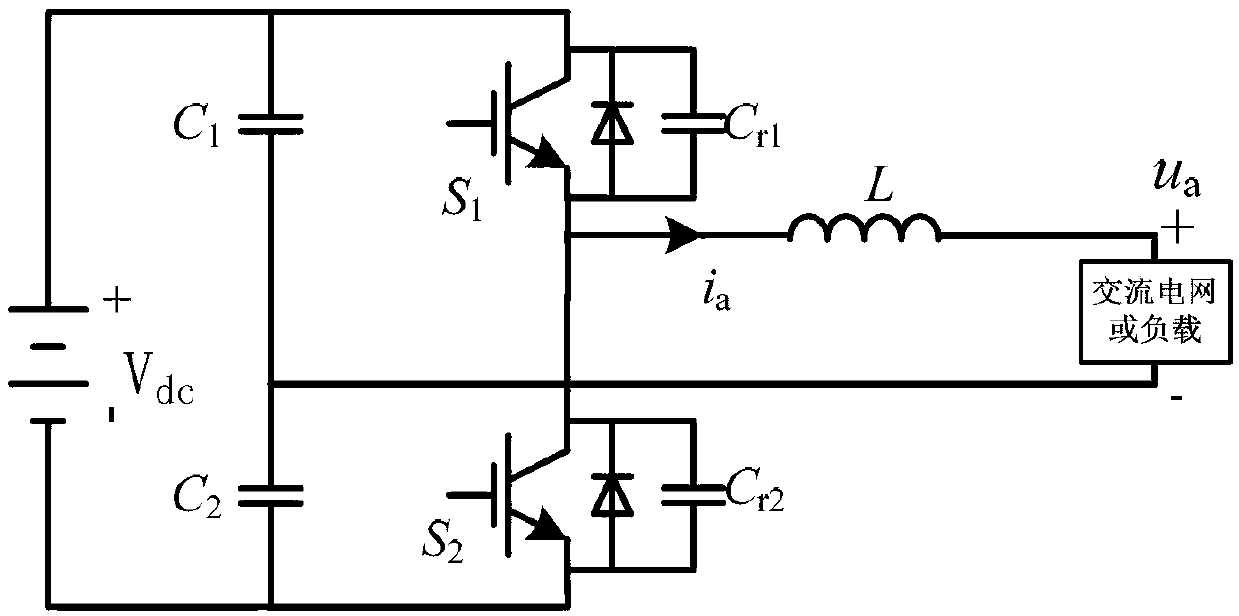
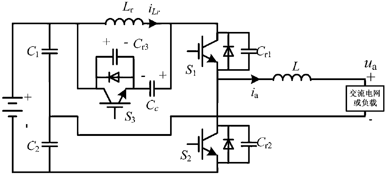
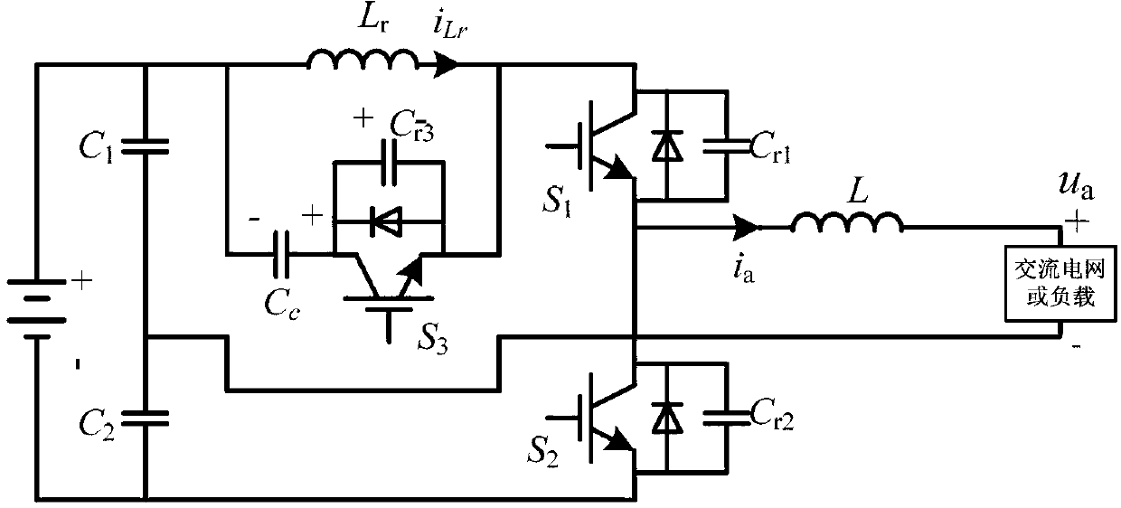
[0025] refer to figure 2 , the low additional voltage stress zero-voltage switch battery energy storage half-bridge inverter of the present invention includes a DC side battery, a DC side voltage dividing capacitor C 1 ~C 2 , by two fully controlled main switches S with anti-parallel diodes 1 ~S 2 The single-phase bridge arm is connected to the output filter inductance L between the midpoint of the bridge arm and the AC grid or AC load, where: the two main switches S of the single-phase bridge arm 1 ~S 2 Parallel capacitor C r1 ~C r2 , in the inverter DC voltage divider capacitor C 1 ~C 2 Auxiliary switch S with anti-parallel diode is connected between DC bus and single-phase bridge arm 3 with clamp capacitor C c The series branch of the auxiliary switch S 3 Parallel capacitance across both ends of the C r3 , auxiliary switch S 3 with clamp capacitor C c The resonant inductance L is connected across the two ends of the series branch composed of r.
[0026] figure 2 In the specific embodiment shown, the auxiliary switch S 3 The collector is connected to the positive terminal of the battery on the DC side of the inverter, and the emitter is connected to the clamp capacitor C c The other end of the clamp capacitor Cc is connected to the positive bus bar of the single-phase bridge arm, and the resonant inductor L r One end is connected to the positive terminal of the battery on the DC side of the inverter, and the other end is connected to the positive busbar of the single-phase bridge arm.
[0027] image 3 As shown in another embodiment, the auxiliary switch S 3 collector and clamp capacitor C c The emitter is connected to the positive bus of the single-phase bridge arm, the other end of the clamping capacitor Cc is connected to the positive end of the battery on the DC side of the inverter, and the resonant inductance L r One end is connected to the positive terminal of the battery on the DC side of the inverter, and the other end is connected to the positive busbar of the single-phase bridge arm.
[0028] Figure 4 As shown in another embodiment, the auxiliary switch S 3 The collector is connected to the negative bus bar of the single-phase bridge arm, and the collector is connected to the clamp capacitor C c The other end of the clamping capacitor Cc is connected to the negative end of the battery on the DC side of the inverter, and the resonant inductance L r One end is connected to the negative terminal of the battery on the DC side of the inverter, and the other end is connected to the negative busbar of the single-phase bridge arm.
[0029] Figure 5 As shown in another embodiment, the auxiliary switch S3 collector and clamp capacitor C c The emitter is connected to the negative terminal of the battery on the DC side of the inverter, the other end of the clamping capacitor Cc is connected to the negative bus bar of the single-phase bridge arm, and the resonant inductance L r One end is connected to the positive terminal of the battery on the DC side of the inverter, and the other end is connected to the positive busbar of the single-phase bridge arm.
[0030] No additional voltage ZVS half-bridge inverter adopts SPWM modulation.
[0031] SPWM is divided into unipolar and bipolar. During bipolar modulation, S1 and S2 are complementary conduction in the entire modulation wave cycle. The present invention uses bipolar modulation.
[0032] Let the sinusoidal modulation voltage be u ref =msin(ωt), when using bipolar modulation, the duty cycle of switch S1 D = 1 2 [ 1 + m sin ( ωt ) ] , Switch S2 Duty Cycle D = 1 2 [ 1 + m sin ( ωt ) ] .
[0033] For the working process of the zero-voltage switching half-bridge inverter without additional voltage, here is the figure 2 The zero-voltage-switching half-bridge inverter with no additional voltage shown is analyzed separately when the DC bus current flows from the DC side to the AC side and a switching cycle when the DC bus current flows from the AC side to the DC side.
[0034] When the DC bus current flows from the DC side to the AC side, the switching pulse control sequence of the inverter is as follows: Figure 7 shown. In a switching duty cycle, the inverter has 9 working states in total. Figure 8 to Figure 16 It is the working equivalent circuit of one switching cycle when the DC bus energy flows from the storage battery on the DC side to the AC side in the present invention. The main voltage and current waveforms at work are shown in Figure-17.
[0035] Phase 1(t 0 -t 1 ):
[0036] like Figure 8 As shown, the main switch S 2 and auxiliary switch S 3 In the ON state, the main switch S 1 off, the load current through S 2 Anti-parallel diode freewheeling.
[0037] Phase 2(t 1 -t 2 ):
[0038] like Figure 9 shown, t 1 Always turn off S 3. Inductance L r and capacitance C r3 、C r1 resonance, capacitance C r3 The voltage across both ends increases, and the capacitor C r1 The voltage across both ends decreases.
[0039] Phase 3(t 2 -t 3 ):
[0040] like Figure 10 shown, t 2 time, the capacitance C r1 voltage decreases to zero, the main switch S 1 The reverse diode conducts and the resonance ends.
[0041] Phase 4(t 3 -t 4 ):
[0042] like Figure 11 shown, t 3 moment, s 1 Zero voltage turn on. Main switch S 1 with S 2 anti-parallel diode commutation, due to L r The presence of the main switch S 2 The reverse recovery process of the antiparallel diode is suppressed.
[0043] Stage 5(t 4 -t 5 ):
[0044] like Figure 12 shown, t 4 time, the commutation ends, the main switch S 2 The antiparallel diode current is reduced to zero. At this time, in order to realize soft switching, zero-voltage turn-on S 2 , bridge arm through, for L r Magnetizing.
[0045] Stage 6(t 5 -t 6 ):
[0046] like Figure 13 shown, t 5 moment, turn off the main switch S 2. Inductance L r and capacitance C r3 、C r2 resonance, capacitance C r2 The voltage across both ends increases, and the capacitor C r3 The voltage across both ends decreases.
[0047] Stage 7(t 6 -t 7 ):
[0048] like Figure 14 shown, t 6 time, the capacitance C r3 voltage decreases to zero, the main switch S 3 The reverse diode conducts and the resonance ends. Auxiliary switch S 3 Zero voltage turn on.
[0049] Stage 8(t 7 -t 8 ):
[0050] like Figure 15 shown, t 7 moment, the main switch S 1 off. load current to capacitor C r2 discharge, giving the capacitor C r1 Charge.
[0051] Stage 9(t 8 -t 9 ):
[0052] like Figure 16 shown, t 9 time, the capacitance C r1 voltage increases to V dc; Capacitance C r2 voltage decreases to zero, the load current passes through the main switch S 2 Anti-parallel diode freewheeling. Main switch S 2 Zero voltage is turned on, the circuit state is the same at time t0 at time t9, and the next cycle is repeated.
[0053] When the DC bus current flows from the AC side to the DC side, the switching pulse control sequence of the inverter is as follows: Figure 18 shown. In a switching duty cycle, the inverter has 9 working states in total. Figure 19 ~ Figure 27 It is the working equivalent circuit of one switching cycle when the DC bus energy flows from the AC side to the DC side battery. The main voltage and current waveforms during operation are as Figure 28 shown.
[0054] Phase 1(t 0 -t 1 ):
[0055] like Figure 19 As shown, the main switch S 1 and auxiliary switch S 3 In the ON state, the main switch S 2 off, the load current through S 1 Anti-parallel diode freewheeling.
[0056] Phase 2(t 1 -t 2 ):
[0057] like Figure 20 shown, t 1 Always turn off S 3 , due to the presence of parallel capacitors, S 3 Zero voltage shutdown. Inductance L r and capacitance C r3 、C r2 resonance, capacitance C r3 The voltage across both ends increases, and the capacitor C r2 The voltage across both ends decreases.
[0058] Phase 3(t 2 -t 3 ):
[0059] like Figure 21 shown, t 2 time, the capacitance C r2 voltage decreases to zero, the main switch S 2 The reverse diode conducts and the resonance ends.
[0060] Phase 4(t 3 -t 4 ):
[0061] like Figure 22 shown, t 3 moment, the main switch S 2 Zero voltage turn on. Main switch S 2 with S 1 anti-parallel diode commutation, due to L r The presence of the main switch S 1 The reverse recovery process of the antiparallel diode is suppressed.
[0062] Stage 5(t 4 -t 5 ):
[0063] like Figure 23 shown, t 4 time, the commutation ends, the main switch S 1 The antiparallel diode current is reduced to zero. At this time, in order to realize soft switching, the main switch S is turned on at zero voltage 1 , bridge arm through, for L r Magnetizing.
[0064] Stage 6(t 5 -t 6 ):
[0065] like Figure 24 shown, t 5 time, turn off the main switch S 1. Inductance L r and capacitance C r3 、C r1 resonance, capacitance C r1 The voltage across both ends increases, and the capacitor C r3 The voltage across both ends decreases.
[0066] Stage 7(t 6 -t 7 ):
[0067] like Figure 25 shown, t 6 time, the capacitance C r3 voltage decreases to zero, the auxiliary switch S 3 The reverse diode conducts and the resonance ends. Auxiliary switch S 3 Zero voltage turn on.
[0068] Stage 8(t 7 -t 8 ):
[0069] like Figure 26 shown, t 7 moment, the main switch S 2 off. load current to capacitor C r1 discharge, giving the capacitor C r2 Charge.
[0070] Stage 9(t 8-t 9 ):
[0071] like Figure 27 shown, t 8 time, the capacitance C r2 voltage increases to V dc; Capacitance C r1 voltage decreases to zero, the load current passes through the main switch S 1 Anti-parallel diode freewheeling. Main switch S 1 Zero voltage is turned on, the circuit state is the same at time t0 at time t9, and the next cycle is repeated.
[0072] The above is a preferred embodiment of the present invention, for Figure 3-5 The embodiment shown, its specific implementation is the same as the above-mentioned figure 2 The illustrated embodiments are similar and will not be described in detail.
[0073] Specific embodiments of the present invention have been described above. It should be understood that the present invention is not limited to the specific embodiments described above, and those skilled in the art may make various changes or modifications within the scope of the claims, which do not affect the essence of the present invention.

PUM

no PUM

Description & Claims & Application Information

We can also present the details of the Description, Claims and Application information to help users get a comprehensive understanding of the technical details of the patent, such as background art, summary of invention, brief description of drawings, description of embodiments, and other original content. On the other hand, users can also determine the specific scope of protection of the technology through the list of claims; as well as understand the changes in the life cycle of the technology with the presentation of the patent timeline. Login to view more.

Similar technology patents

Classification and recommendation of technical efficacy words

  • Simple structure
  • Reverse recovery inhibition

Microlithographic projection exposure apparatus

InactiveUS20050068499A1Simple structureReliable and low-maintenance operationProjectorsPhotomechanical exposure apparatusCamera lensPhysics
Owner:CARL ZEISS SMT GMBH
Why Eureka
Try Eureka