Minimum-voltage, active-clamp and three-phase grid-connected inverter

An inverter and voltage technology, which is applied in electrical components, conversion devices for converting AC power input to DC power output, and output power, etc. The effect of improving power density, improving circuit efficiency, and increasing operating frequency

Inactive Publication Date: 2010-07-21
ZHEJIANG UNIV
3 Cites 12 Cited by

AI-Extracted Technical Summary

Problems solved by technology

This kind of three-phase inverter can realize the function of grid-connected power generation, but the circuit works in a hard switching state, there is a problem of reverse recovery of the diod...

Abstract

The invention discloses a minimum-voltage, active-clamp and three-phase grid-connected inverter, which comprises a DC inverter power supply, an AC filter inductor and a three-phase bridge arm. The three-phase bridge arm consists of 6 full-control master switches with anti-parallel diodes, an auxiliary switch with an anti-parallel diode is connected between the DC inverter power supply and the DC bus of the three-phase bridge arm, the two ends of the master switches and the auxiliary switch are all connected with a capacitor in parallel, and the two ends of the auxiliary switch are bridged with a resonance branch formed by serial connection of a resonance inductor and a clamp capacitor. The inverter of the invention has simple structure and adopts an improved space vector modulation method. When the power-factor angle of the grid-connected current of the inverter is between minus 30 degrees and plus 30 degrees , the zero-voltage switching-on of all the master switches can be realized through one action of the auxiliary switch in each switching period, the reverse recovery current of the anti-parallel diodes of the master switches are inhibited, and the switch voltage stress is equal to the voltage of the DC inverter power supply. Moreover, due to the low switching loss and high circuit efficiency, the invention facilitates the improvement of the operating frequency, thereby enhancing the power density.

Application Domain

Technology Topic

Three-phasePower density +13

Image

  • Minimum-voltage, active-clamp and three-phase grid-connected inverter
  • Minimum-voltage, active-clamp and three-phase grid-connected inverter
  • Minimum-voltage, active-clamp and three-phase grid-connected inverter

Examples

  • Experimental program(1)

Example Embodiment

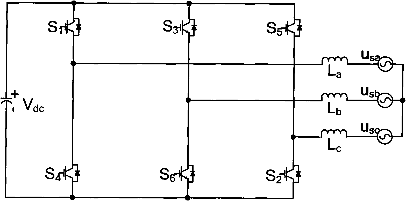
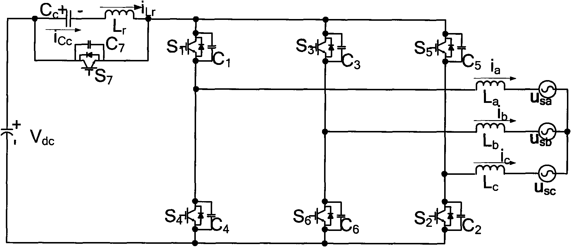
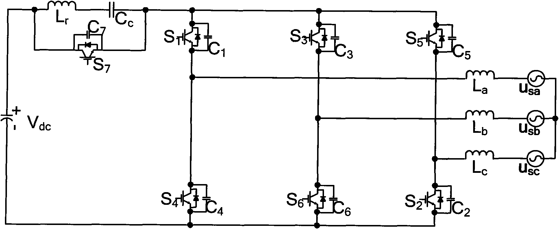
[0015] refer to figure 2 , the minimum voltage active clamp three-phase grid-connected inverter of the present invention includes the power supply V on the DC side of the inverter dc , consisting of six fully controlled main switches S with anti-parallel diodes 1 ~S 6 The three-phase bridge arms formed are respectively connected to the output filter inductance L between the midpoint of each phase bridge arm and the AC grid a ~ L c , which is characterized by the six main switches S of the three-phase bridge arm 1 ~S 6 Parallel capacitor C 1 ~C 6 , power supply V on the DC side of the inverter dc Auxiliary switch S with anti-parallel diode is connected between DC bus and three-phase bridge arm 7 , auxiliary switch S 7 Parallel capacitance across both ends of the C 7 , and at the auxiliary switch S 7 Connected across both ends by the resonant inductor L r with clamp capacitor C c series resonant branch.
[0016] figure 2 In the specific example shown, the auxiliary switch S 7 The collector is connected to the positive terminal of the inverter DC power supply, the emitter is connected to the positive busbar of the three-phase bridge arm, and the resonant inductance L r Connected to the positive bus bar of the three-phase bridge arm, the clamp capacitor C c Connect to the positive terminal of the inverter DC power supply. image 3 In the example shown, the auxiliary switch S 7 The collector is connected to the positive terminal of the inverter DC power supply, the emitter is connected to the positive bus bar of the three-phase bridge arm, and the clamping capacitor C c Connected with the positive bus bar of the three-phase bridge arm, the resonant inductance L r Connect to the positive terminal of the inverter DC power supply. Figure 4 In the example shown, the auxiliary switch S 7 The emitter is connected to the negative terminal of the inverter DC power supply, the collector is connected to the negative bus bar of the three-phase bridge arm, and the clamp capacitor C c Connected with the negative bus bar of the three-phase bridge arm, the resonant inductance L r Connect to the negative terminal of the inverter DC power supply. Figure 5 In the example shown, the auxiliary switch S 7 The emitter is connected to the negative terminal of the inverter DC power supply, the collector is connected to the negative bus bar of the three-phase bridge arm, and the resonant inductance L r Connected to the negative bus bar of the three-phase bridge arm, the clamp capacitor C c Connect to the negative terminal of the inverter DC power supply.
[0017] Minimum voltage active clamp three-phase grid-connected inverter adopts space vector control. In a grid voltage power frequency cycle, the control of the inverter can be divided into 12 sectors, and the division of grid voltage and current sectors is as follows: Image 6 shown. Image 6 Phase A grid voltage u sa Cosine wave at 0° to 30° is voltage sector 2, phase A grid voltage u sa The cosine wave at 30° to 60° is the voltage sector 3, and so on, the phase A grid voltage u sa Cosine wave at 300° to 330° is voltage sector 12, phase A grid-connected current i a Cosine wave at 0° to 30° is current sector 2, phase A grid-connected current i a The cosine wave at 30° to 60° is the current sector 3, and so on, the phase A grid-connected current i a The cosine wave is the current sector 12 at 300° to 330°. Figure 7 Shown is the grid voltage space vector diagram, in the figure arrive Indicates the inverter switching vector, switching vector Indicates the inverter main switch S 2 , S 4 , S 6 Conduction, inverter main switch S 1 , S 3 , S 5 cutoff, switch vector Indicates the inverter main switch S 1 , S 2 , S 6 Conduction, inverter main switch S 3 , S 4 , S 5 cutoff, and so on, switch vector Indicates the inverter main switch S 1 , S 3 , S 5 Conduction, inverter main switch S 2 , S 4 , S 6 due. Inverter Switching Vector and Indicates zero vector, inverter switching vector and Represents a nonzero vector. The switching pulse control sequence of the inverter grid-connected current in different grid voltage sectors is shown in Table 1. Table 1 shows the inverter main switch vector switching sequence corresponding to different grid voltage sectors and grid-connected current sectors .
[0018] Table 1
[0019]
[0020] The minimum voltage active clamp inverter adopts a special space vector modulation strategy, and each grid voltage power frequency cycle is divided into 12 space vector sectors, and the absolute value of the AC grid-connected current of one phase is kept at the maximum in each sub-sector . The bridge arm switch that flows through the phase with the largest absolute value of current does not commutate. If the direction of the phase with the largest absolute value of the output filter inductor current is positive, the zero vector is If the absolute value of the current maximum phase direction is negative, then the zero vector is The switching sequence of the space vector ensures that the absolute value of the instantaneous output current of the inverter is small when the grid is connected to the grid. In the two-phase switching commutation, there is a diode reverse recovery. The two commutations are aligned in time, and the auxiliary circuit only needs to create the bus voltage once. The chance of resonating to zero can realize the zero-voltage turn-on of the two switches. When the grid-connected current power factor angle of the inverter is between plus and minus 30°, the zero-voltage turn-on of the inverter can be realized. The six main switches S in the inverter 1 ~S 6 and auxiliary switch S 7 Controlled by a space vector PWM controller with a fixed switching frequency, the auxiliary switch S 7 Switching frequency and fully controlled main switch S 1 ~S 6 same as the switching frequency, the auxiliary switch S 7 Only in inverter main switch S 1 ~S 6 Shutdown for brief periods of switching from zero vector to non-zero vector.
[0021] For the minimum voltage active clamp three-phase grid-connected inverter, in the 12 sectors of a power frequency cycle of the grid-connected current, the inverter control is similar, here we use figure 2 The minimum voltage active clamp three-phase grid-connected inverter shown in the example is analyzed for a switching cycle in the grid-connected current sector 2. If the grid-connected current power factor angle of the inverter is 0°, the grid voltage and There is no phase angle difference corresponding to the grid-connected current of the phase, and the pulse control sequence of the inverter switching in sector 2 is as follows: Figure 8 shown. In a switching duty cycle, the inverter has 8 working states in total. The main voltage and current waveforms during operation are as Figure 9 shown.
[0022] Phase 1(t 0 -t 1 ):
[0023] Main switch S 1 , S 3 , S 5 and auxiliary switch S 7 is in the conduction state. by the resonant inductance L r , the clamp capacitor C c and auxiliary switch S 7 In the formed resonant circuit, the current of the resonant inductance Lr increases linearly.
[0024] Phase 2(t1 -t 2 ):
[0025] t 1 moment, the auxiliary switch S 7 turn off, the resonant inductance L r to the main switch S 2 , S 4 , S 6 The shunt capacitor C 2 , C 4 , C 6 discharge, to the auxiliary switch S 7 The shunt capacitor C 7 charging, S 7 Zero voltage shutdown. to t 2 moment, the three main switches S 2 , S 4 , S 6 The shunt capacitor C 2 , C 4 , C 6 voltage resonates to zero, the main switch S 2 , S 4 , S 6 The antiparallel diode starts to conduct, the resonant inductor L r voltage is clamped to the inverter power supply voltage V dc. to t 2 moment, the resonant inductance L r and main switch S 2 , S 4 , S 6 The shunt capacitor C 2 , C 4 , C 6 , auxiliary switch S 7 The shunt capacitor C 7 Resonance completes, the main switch S 2 , S 6 Can achieve zero voltage turn-on.
[0026] Phase 3(t 2 -t 3 ):
[0027] At this stage, the main switch S 3 and S 5 The antiparallel diode undergoes a reverse recovery process due to the resonant inductance L r presence of the main switch S 3 and S 5 The antiparallel diode reverse recovery current is suppressed. At time t3, the main switch S 3 and S 5 The antiparallel diode current becomes zero.
[0028] Phase 4(t 3 -t 4 ):
[0029] At time t3, the main switch S 3 and S 5 The antiparallel diode is turned off, the resonant inductance L r Start and main switch S 3 , S 4 , S 5 The shunt capacitor C 3 , C 4 , C 5 , auxiliary switch S 7 The shunt capacitor C 7 resonance, the main switch S 3 , S 4 , S 5 Capacitance at both ends C 3 , C 4 , C 5 voltage starts to increase, the auxiliary switch S 7 Parallel capacitor C at both ends 7 The voltage decreases, and at time t4, S 7 Parallel capacitor C at both ends 7 voltage decreases to zero, S 7 Anti-parallel diode conduction, S 7 Realize zero voltage turn-on.
[0030] Stage 5(t 4 -t 5 ):
[0031] to t 4 moment, the circuit enters the switch vector 100 state, the main switch S 1 , S 6 , S 2 and auxiliary switch S 7 conduction. by the resonant inductance L r , the clamp capacitor C c and auxiliary switch S 7 In the closed loop formed, the current of the resonant inductor Lr increases linearly.
[0032] Stage 6(t 5 -t 6 ):
[0033] At time t5, the main switch S 6 turn off, the filter inductor L b The current in the main switch S 6 The shunt capacitor C 6 charging, to the main switch S 3 The shunt capacitor C 3 discharge, due to S 6 The presence of parallel capacitors, S 6 Realize zero voltage turn off.
[0034] Stage 7(t 6 -t 7 ):
[0035] At time t6, the circuit enters the switch vector 110 state, the main switch S 1 , S 3 , S 2 and auxiliary switch S 7 conduction. by the resonant inductance L r , the clamp capacitor C c and auxiliary switch S 7 In the closed loop formed, the current of the resonant inductor Lr increases linearly.
[0036] Stage 8(t 7 -t 8 ):
[0037] At time t7, the main switch S 2 turn off, the filter inductor L c The current in the main switch S 2 The shunt capacitor C 2 charging, to the main switch S 5 The shunt capacitor C 5 discharge, due to S 2 The presence of parallel capacitors, S 2 Realize zero voltage turn off. At time t8, S 2 off, the main switch S 5 body diode conducts, coinciding with Phase 1. The circuit repeats for the next cycle.

PUM

no PUM

Description & Claims & Application Information

We can also present the details of the Description, Claims and Application information to help users get a comprehensive understanding of the technical details of the patent, such as background art, summary of invention, brief description of drawings, description of embodiments, and other original content. On the other hand, users can also determine the specific scope of protection of the technology through the list of claims; as well as understand the changes in the life cycle of the technology with the presentation of the patent timeline. Login to view more.

Similar technology patents

Classification and recommendation of technical efficacy words

  • Simple structure
  • Reverse recovery inhibition

Microlithographic projection exposure apparatus

InactiveUS20050068499A1Simple structureReliable and low-maintenance operationProjectorsPhotomechanical exposure apparatusCamera lensPhysics
Owner:CARL ZEISS SMT GMBH
Why Eureka
Try Eureka