

A high-speed sense amplifier circuit of an SRAM type memory
A technology of sense amplifier and memory, applied in static memory, digital memory information, information storage and other directions, can solve the problems of large input voltage difference and affect the reading speed of memory, reduce the requirement of input voltage difference and improve the response speed and processing power, the effect of speeding up the reading of "0"
- Summary
- Abstract
- Description
- Claims
- Application Information
AI Technical Summary
Problems solved by technology
Method used
Image


Examples
Embodiment Construction
[0023] Below in conjunction with accompanying drawing and concrete implementation the present invention is described in further detail:
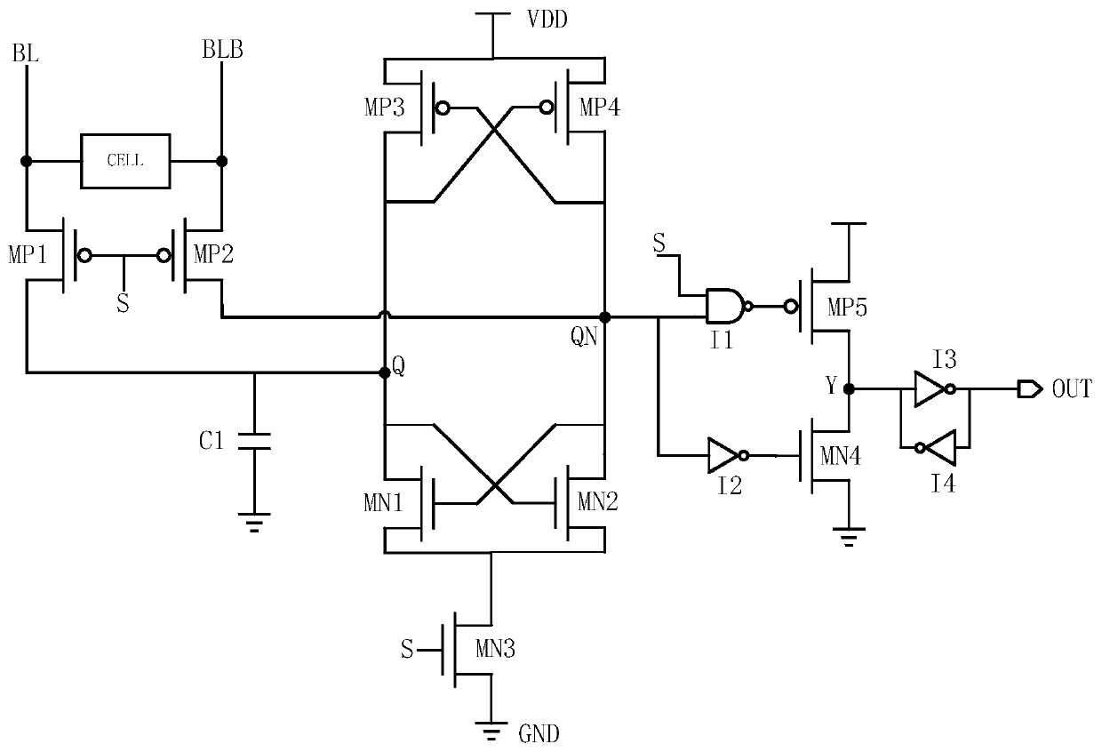
[0024] Such as figure 1 Shown is the circuit structure diagram of the high-speed sense amplifier of the SRAM type memory of the present invention. Consists of: bit line read switch module, latch type amplifier module and output module. The bit line read switch module includes PMOS transistors MP1, MP2, capacitor C1; the latch type amplifier module includes PMOS transistors MP3, MP4, NMOS transistors MN1, MN2, MN3; the read module includes NAND gate I1, inverter I2 -I4, PMOS transistor MP5, NMOS transistor MP4.
[0025] The source terminals of the PMOS transistors MP1 and MP2 in the bit line read switch module are respectively connected to the SRAM unit bit line (CELL) output BL and BLB terminals, and the gate terminals of the PMOS transistors MP1 and MP2 are connected in common, controlled by the read enable input signal S, and the drain ...
PUM
 Abstract
Description
Claims
Application Information