Semiconductor structures and methods of forming them

A semiconductor and substrate technology, applied in the field of semiconductor structure and its formation, can solve the problems that the performance of semiconductor structure needs to be improved

Active Publication Date: 2021-12-14
SEMICON MFG INT (SHANGHAI) CORP +1
View PDF10 Cites 0 Cited by
  • Summary
  • Abstract
  • Description
  • Claims
  • Application Information

AI Technical Summary

Problems solved by technology

[0004] However, despite the introduction of germanium in the channel material, the performance of semiconductor structures still needs to be improved

Method used


Image

  • Semiconductor structures and methods of forming them
  • Semiconductor structures and methods of forming them
  • Semiconductor structures and methods of forming them

Examples


Embodiment Construction

[0033] It can be seen from the background art that the performance of existing semiconductor structures still needs to be improved.

[0034] Now combined with a method of forming a semiconductor structure for analysis, figure 1 and figure 2 It is a schematic structural diagram corresponding to a method for forming a semiconductor structure, and the process steps for forming a semiconductor structure include:

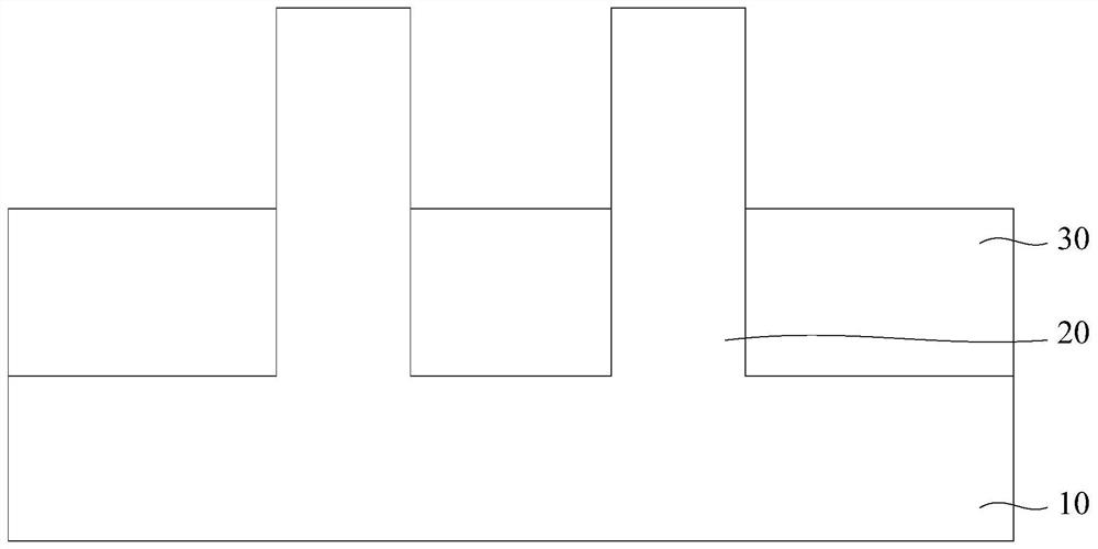
[0035] refer to figure 1 , providing a substrate 10 and a fin 20 protruding from the substrate 10, the substrate 10 has an isolation layer 30 covering part of the sidewall of the fin 20, and the top of the isolation layer 30 is lower than the The top of the fin 20.

[0036] Wherein, the material of the fin portion 20 is silicon germanium.

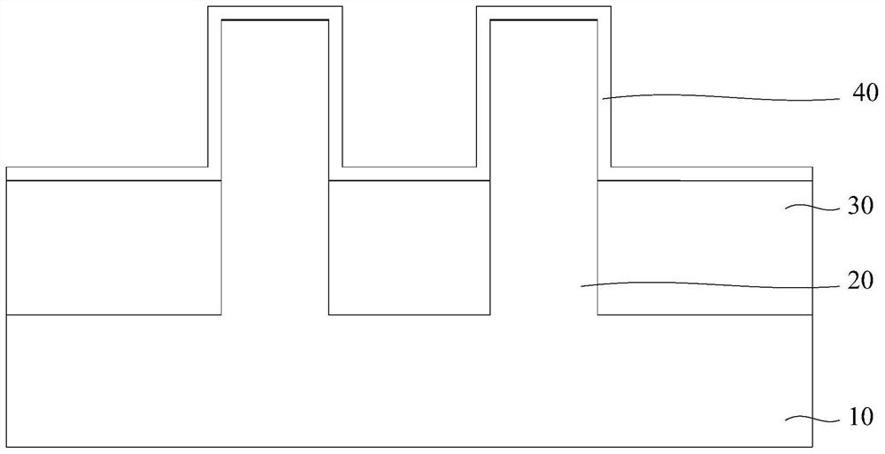
[0037] refer to figure 2 A thermal oxidation process is used to form a gate oxide layer 40 on the top and sidewalls of the fin portion 20 exposed by the isolation layer 30 .

[0038] The gate oxide layer 40 serves as a gate ...


PUM


Abstract

A semiconductor structure and its forming method, the forming method comprising: providing a substrate and fins protruding from the substrate, the material of the fins contains germanium, the substrate has an isolation layer covering the side walls of the fins, and isolating The top of the layer is lower than the top of the fin; an atomic layer deposition process is used to form a dummy gate oxide layer on the top and side walls of the fin exposed by the isolation layer, and the process temperature of the atomic layer deposition process is the first temperature; a dummy gate oxide layer across the fin is formed. Gate, the dummy gate covers the surface of the dummy gate oxide layer; a dielectric layer is formed on the isolation layer, the dielectric layer covers the sidewall of the dummy gate and exposes the top of the dummy gate; removes the dummy gate and dummy gate oxide layer, exposing the top of the fin and part of the sidewall ; Forming an interface layer on the exposed top and sidewall of the fin, the process temperature for forming the interface layer is a second temperature, and the second temperature is less than or equal to the first temperature. The invention can prevent the germanium element in the fin from diffusing into the interface layer, thereby improving the interface characteristics between the interface layer and the fin, and enhancing carrier mobility.

Description

technical field [0001] The invention relates to the technical field of semiconductor manufacturing, in particular to a semiconductor structure and a forming method thereof. Background technique [0002] Carrier mobility is a measure of the overall movement of electrons and holes within a semiconductor structure. The carrier mobility has an important influence on the electrical properties of the semiconductor structure: on the one hand, the carrier mobility determines the conductivity of the semiconductor material, the greater the carrier mobility, the greater the conductivity, so when the same current passes through , the smaller the power consumption. On the other hand, the carrier mobility affects the operating frequency of the semiconductor structure. The greater the carrier mobility, the shorter the time for carriers to cross the base region, so the frequency response characteristics of the semiconductor structure are more excellent. [0003] Studies have found that co...

Claims


Application Information

Patent Timeline
Patent Type & Authority Patents(China)
IPC IPC(8): H01L21/336H01L29/78
Inventor 周飞
Owner SEMICON MFG INT (SHANGHAI) CORP
Why Eureka
Try Eureka