Semiconductor structures and methods of forming them

A semiconductor and gate structure technology, applied in the field of semiconductor structure and its formation, can solve problems such as floating gate defects and semiconductor structure performance degradation, so as to reduce the probability of over-etching and improve performance

Active Publication Date: 2021-03-09
SEMICON MFG INT (SHANGHAI) CORP +1
View PDF6 Cites 0 Cited by
  • Summary
  • Abstract
  • Description
  • Claims
  • Application Information

AI Technical Summary

Problems solved by technology

[0005] However, in the prior art, the floating gate formed by the self-aligned polysilicon process is prone to defects, which leads to the degradation of the performance of the formed semiconductor structure.

Method used


Image

  • Semiconductor structures and methods of forming them
  • Semiconductor structures and methods of forming them
  • Semiconductor structures and methods of forming them

Examples


Embodiment Construction

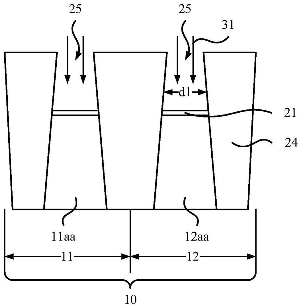
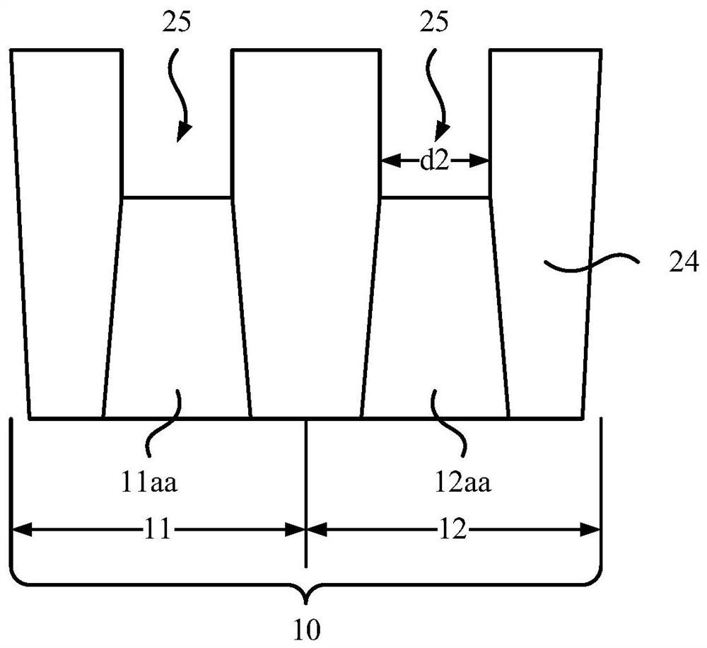
[0018] It can be seen from the background art that defects are prone to appear in the floating gate formed by introducing the self-aligned polysilicon process in the prior art, thereby affecting the performance of the formed semiconductor structure. Combining with the formation process of a semiconductor structure that introduces a self-aligned polysilicon process to form a floating gate, the cause of the floating gate defect problem is analyzed:

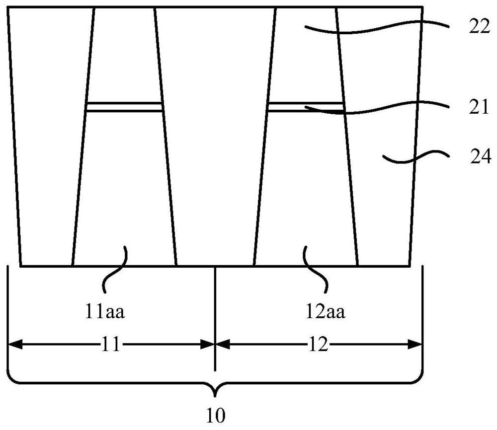
[0019] refer to Figure 1 to Figure 5 , shows a schematic cross-sectional structure corresponding to each step of a method for forming a semiconductor structure.

[0020] refer to figure 1 , provide a substrate 10, the substrate 11 includes a high voltage region 11 and a core region 12; an isolation structure 24, the isolation structure 24 is located in the substrate 10 of the core region 12 and the high voltage region 11, in the A core active region 12aa is defined in the substrate 10 of the core region 12, and a high-voltage act...


PUM


Abstract

A semiconductor structure and a method for forming the same, comprising: providing a substrate, the substrate including a core region and a high voltage region, a pad oxide layer is formed on the core region and the high voltage region; removing the pad oxide layer; removing the After the pad oxide layer, form a first dielectric layer at least on the high voltage region; form a hard mask layer on the first dielectric layer; use the hard mask layer as a mask, in the core area and an isolation structure is formed in the high voltage region. Removing the pad oxide layer before the formation of the isolation structure can effectively reduce the number of times the wet etching process is used after the subsequent formation of the isolation structure, which is conducive to reducing the probability of bridging and short-circuit problems, and reducing the subsequent formation of gates. The probability of defects in the pole structure is conducive to the improvement of the performance of the formed semiconductor structure.

Description

technical field [0001] The invention relates to the field of semiconductor manufacturing, in particular to a semiconductor structure and a forming method thereof. Background technique [0002] In the current semiconductor industry, integrated circuits can be divided into three main types: analog circuits, digital circuits, and digital / analog hybrid circuits. Among them, memory devices are an important type in digital circuits. Among storage devices, in recent years, flash memory (Flash Memory, referred to as a flash memory device) has attracted attention from all parties and has developed particularly rapidly. The main feature of the flash memory device is that it can keep storing information for a long time without power on; it also has the advantages of high integration, fast storage speed, and easy erasing and rewriting. Therefore, flash memory devices have been widely used in many fields such as personal computers and automatic control. [0003] With the continuous de...

Claims


Application Information

Patent Timeline
Patent Type & Authority Patents(China)
IPC IPC(8): H01L27/11521
Inventor 陈勇
Owner SEMICON MFG INT (SHANGHAI) CORP
Why Eureka
Try Eureka