A method for processing the shape of a pcb product with a narrow edge ptfe antenna without internal positioning

A PTFE, shape processing technology, applied in the field of PCB manufacturing, can solve the problems of slow speed, low efficiency, small size does not meet the cleaning requirements of the finished product cleaning machine, etc., to ensure product quality, eliminate large or small size, guarantee Qualified size effect

Active Publication Date: 2021-06-18
HUIZHOU KING BROTHER CIRCUIT TECH +2
View PDF4 Cites 0 Cited by
  • Summary
  • Abstract
  • Description
  • Claims
  • Application Information

AI Technical Summary

Problems solved by technology

[0002] 5G applications will gradually increase from 3GHz to 6GHz or even higher frequency of 30GHz to transmit high-speed signals, which will bring new technical challenges to the manufacture and processing of antenna radio frequency materials
Moreover, because the size of the formed ultra-narrow antenna PCB product is too small to meet the cleaning requirements of the finished product cleaning machine, it can only be wiped manually with alcohol, which is not only slow and inefficient, but also the oxides are not easy to clean.

Method used


Image

  • A method for processing the shape of a pcb product with a narrow edge ptfe antenna without internal positioning
  • A method for processing the shape of a pcb product with a narrow edge ptfe antenna without internal positioning
  • A method for processing the shape of a pcb product with a narrow edge ptfe antenna without internal positioning

Examples


Embodiment Construction

[0025] It should be understood that the specific embodiments described herein are merely intended to illustrate the invention and are not intended to limit the invention.

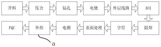
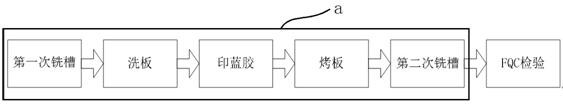
[0026] Such as Figure 1 - Figure 2 In the present invention, the outer shape processing method A of the narrow edge antenna PCB according to an embodiment of the present invention can be applied to the manufacturer of the conventional narrow edge antenna PCB, widely used, and is very versatile. A narrow antenna PCB shape processing method A, including the following steps:

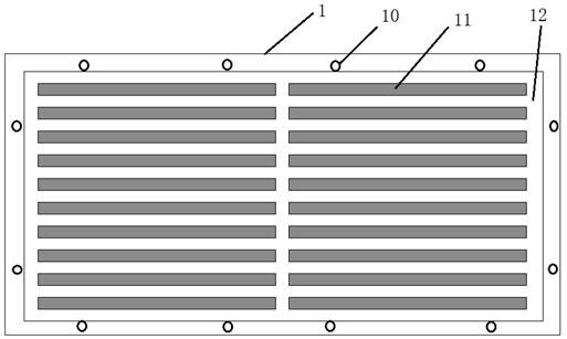
[0027] S1: image 3 As shown, 20 antenna PCB11 is arranged on a matrix, and the upper and lower adjacent antenna PCB11 is disposed as a unit 2, and the antenna PCB11 is surrounded by the portion 12, at the position of the largeboard body 1. Set the positioning hole 10;

[0028] S2: The first milling groove is used to process the processing unit 12 on the large plate body 1 by the CNC machine tool, and the machining direction of the milling gr...


PUM


Abstract

The invention discloses a shape processing method for a narrow-side PTFE antenna PCB product without internal positioning, which is suitable for an ultra-narrow antenna PCB made of PTFE materials, and can ensure that the antenna PCB board is qualified in size after shape processing, and has no oxide and burr defects. Guarantee product quality and eliminate defects of oversized or undersized dimensions due to shape processing.

Description

Technical field [0001] The present invention relates to the field of PCB manufacturing, and more particularly to an outer shape processing method of a narrow sideless non-internal positioning PTFE material antenna PCB product. Background technique [0002] The 5G application will gradually rise from 3GHz to 30 GHz, 30GHz, to transmit high-speed signals, which will bring new technical challenges to the manufacture and processing of antenna RF materials. PTFE has excellent dielectric properties, chemical resistance and high-temperature resistance, so polytetrafluoroethylene is the most ideal material for processing high-frequency antenna PCB products, due to the number of 5G Massive MIMO antennas and complexity Active antenna system far above the previous 4G requires more products to be integrated in smaller sizes, so higher requirements are also proposed for the processing of materials. [0003] For ordinary rigid printed boards, the traditional circuit boards in the industry have...

Claims


Application Information

Patent Timeline
Patent Type & Authority Patents(China)
IPC IPC(8): H05K3/00
Inventor 武守坤林鹭华聂兴培陈春樊廷慧唐宏华
Owner HUIZHOU KING BROTHER CIRCUIT TECH
Why Eureka
Try Eureka