Silicon through-electrode void-free filling method and copper plating solution used in filling method

A technology of penetrating electrodes and filling methods, which is applied in the field of electroplating of silicon penetrating electrodes, can solve the problems of incomplete plating in the plating process, long time for penetrating electrodes, and occurrence of defects, so as to shorten filling time, reduce voids, The effect of improving reliability

Active Publication Date: 2019-06-07
KOREA INST OF IND TECH
View PDF5 Cites 4 Cited by
  • Summary
  • Abstract
  • Description
  • Claims
  • Application Information

AI Technical Summary

Problems solved by technology

[0004] In this regard, as a method of forming a through-hole electrode on a silicon substrate, according to Korean Laid-Open Patent Publication No. 10-2015-0099392 (hereinafter referred to as reference document 1), it is proposed to form a diffusion prevention layer on copper by electroless plating, and then laminate a copper seed layer. In order to fill TSVs with the method of reference 1, that is, the electroless plating method, it takes a long time to form the through-electrode, and the plating cannot be completely performed in the plating process, and there is a problem that defects occur, so it is necessary to adjust the power supply method

Method used


Image

  • Silicon through-electrode void-free filling method and copper plating solution used in filling method
  • Silicon through-electrode void-free filling method and copper plating solution used in filling method
  • Silicon through-electrode void-free filling method and copper plating solution used in filling method

Examples


preparation example 1

[0105] Under the conditions of Comparative Example 1, only the current application conditions were changed, and the filling experiment was performed under the current application conditions mentioned in Table 4 below. The amount of current consumed in Comparative Example 1 and Preparation Example 1 was the same.

[0106] Table 4

[0107] Current application conditions of Preparation Example 1

[0108] condition

Current Density (ASD)

Current application time (second, s)

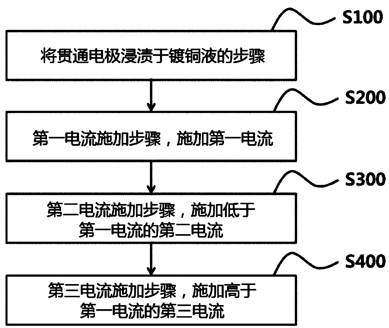
apply the first current

1.1

30

apply the second current

0.2

200

Apply a third current

1.5

620

[0109] (ASD=Ampere per Square Deci-meter, A / dm 2 )

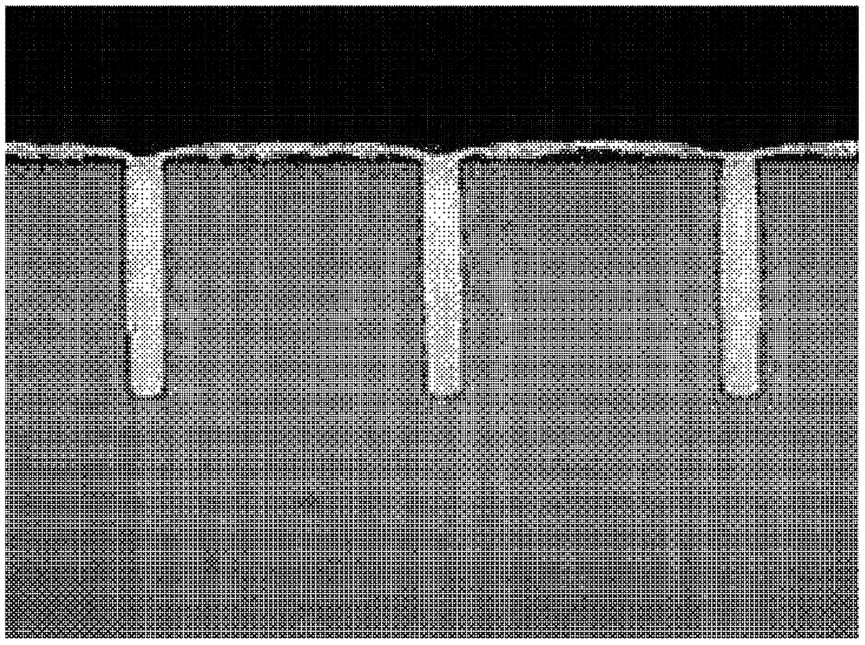
[0110] Figure 5 A cross-section of a via plated by the conditions is shown in . Depend on Figure 5 It was confirmed that in the case of the three-step current application method, the through-holes were filled without defects in the through-electrodes.

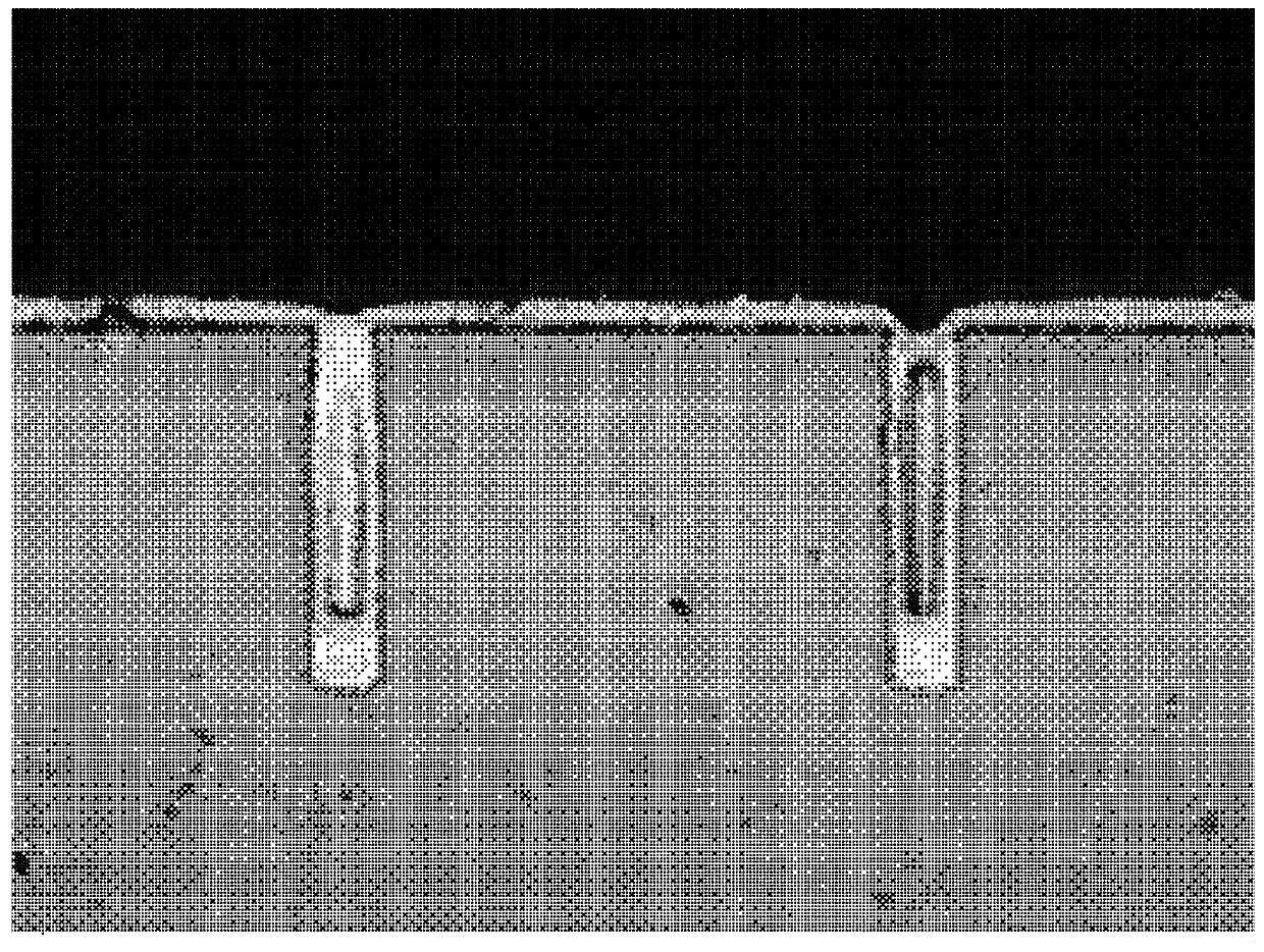
[0111] Further, when comparing Comparative E...


PUM


Abstract

An embodiment of the present invention provides a through-electrode filling method comprising: a step of immersing a through-electrode including a via in a copper plating solution having a leveler anda copper electrolyte; a first current applying step of applying a first current to coat an upper side surface of a via of the through-electrode in the leveler; a second current applying step of applying a second current, the magnitude of which is lower than that of the first current, to form a plating film of the copper electrolyte on the bottom of the via; and a third current applying step of applying a third current, the magnitude of which is higher than that of the first current, to fill with the copper electrolyte in a part from a surface of the plating film of the copper electrolyte to an opening of the via.

Description

technical field [0001] The present invention relates to an electroplating method for through-silicon electrodes, and more specifically relates to a method for filling through-silicon electrodes without defects (voids) in the process of filling the through-silicon electrodes with a plating solution containing a leveler. Background technique [0002] Since the initial stacked package uses metal wires to exchange electrical signals, the operation speed is slow, and because a large number of wires are used, the electrical characteristics of the stacked chips are degraded. In addition, the stacked package requires an additional area on the substrate for wire connection, so the overall size is large, and a gap (gap) for connecting wires is required between the stacked semiconductor chips, so the overall thickness is thick. [0003] In view of this, a package-on-package structure utilizing through electrodes has been proposed in order to overcome the problems of the package-on-pack...

Claims


Application Information

Patent Timeline
Patent Type & Authority Applications(China)
IPC IPC(8): C25D7/12C25D3/38C25D21/12H01L21/768
CPCC25D3/38C25D7/123C25D21/12H01L21/76877
Inventor 李民炯李云英秦祥熏
Owner KOREA INST OF IND TECH
Why Eureka
Try Eureka