Three-dimensional system chip test resource optimization method and system
A system chip and test resource technology, applied in the field of 3D system chip test resource optimization, can solve problems such as not considering test scheduling problems, small test time, etc.
- Summary
- Abstract
- Description
- Claims
- Application Information
AI Technical Summary
Problems solved by technology
Method used
Image

Examples
Embodiment 1
[0063] like figure 1 As shown, a method for optimizing 3D SoC test resources is used to optimize 3D SoC test resources and / or test scheduling, including Step 10: Establishing an STO model based on Stackelberg game theory; Step 11: Establishing a game model; Step 12: Initializing Test strategy; Step 13: Find the optimal test strategy.
[0064] like figure 2 As shown, the STO model established in step 10 includes M resource managers (ResourceManager, RM) and N consumers (Consumer Unit, CU), and the resource manager RM manages test resources, and the Consumers consume test resources, the test resources include the number of available TSVs, test time, test bandwidth, that is, at least two of the number of I / O pins in each layer of the 3D system chip, and the record set L={1,2,... , M}, set V={1,2,...,N}. In the STO model, the optimal test bandwidth allocation is provided for the CU, and all the demands of the CU are provided by the RM. Finally, an equilibrium state is formed ...
Embodiment 2
[0079] A three-dimensional system chip test resource optimization system, including a processor and a storage medium, the storage medium stores a program, the program is designed according to the method for optimizing three-dimensional system chip test resources, and the program is executed when the processor runs Method steps:
[0080] Step 10: Establish an STO model based on Stackelberg game theory;
[0081] Step 11: Establish a game model;
[0082] Step 12: Initialize the test strategy;
[0083] Step 13: Find the optimal testing strategy.
[0084] The program is also used for inputting three-dimensional SoC testing constraints, the testing constraints include at least one of the number of available TSVs and the number of test pins. The program is also used to output an optimal test strategy, and the optimal test strategy includes at least one of a test scheduling strategy and a wafer bandwidth allocation strategy.
Embodiment 3
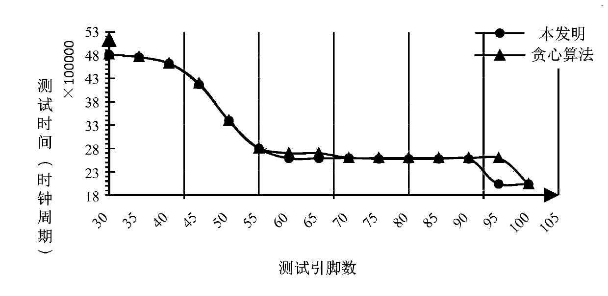
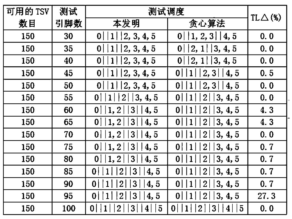
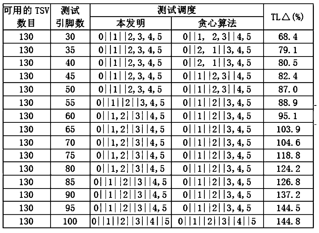
[0086] In order to verify the technical effect of the present invention, the 3D SoC is tested according to the optimal test strategy formed by the present invention, and the test results are compared with the test results of the most mature greedy algorithm and the method proposed by Testrail.
[0087] Firstly, three 3D SoCs are built from d695, f2126, p22810, p34292 and p93791 in ITC'02 (test reference circuit), and they are named 3D SoC1, 3D SoC2 and 3D SoC3 respectively. The specific structure of 3D SoC1 is The reference circuits p93791, p34292, p22810, f2126, and d695 are arranged from top to bottom, and the complexity of the reference circuits is higher as you go upward; the specific structure of 3D SoC2 is to arrange the reference circuits d695, f2126, p22810, p34292, p93791, the lower the reference circuit is, the more complex it is; the specific structure of 3D SoC3 is to arrange reference circuits f2126, p22810, p93791, p34932, and d695 from top to bottom, and the refe...
PUM
 Abstract
Description
Claims
Application Information
 - R&D
- Intellectual Property
- Life Sciences
- Materials
- Tech Scout
- Unparalleled Data Quality
- Higher Quality Content
- 60% Fewer Hallucinations
Browse by: Latest US Patents, China's latest patents, Technical Efficacy Thesaurus, Application Domain, Technology Topic, Popular Technical Reports.
© 2025 PatSnap. All rights reserved.Legal|Privacy policy|Modern Slavery Act Transparency Statement|Sitemap|About US| Contact US: help@patsnap.com