Substrate embedding type three-dimensional system-level packaging method and structure

A system-level packaging and substrate technology, which is applied in semiconductor/solid-state device components, semiconductor devices, electrical components, etc., can solve the problems of serious electromagnetic interference of system-level packaging, aggravating the transmission performance of interconnection structures, and three-dimensional packaging structure integration technology. , to achieve the effects of improving electromagnetic interference performance, realizing miniaturization, and improving packaging integration

Active Publication Date: 2019-06-18
INST OF MICROELECTRONICS CHINESE ACAD OF SCI
View PDF6 Cites 4 Cited by
  • Summary
  • Abstract
  • Description
  • Claims
  • Application Information

AI Technical Summary

Problems solved by technology

[0004] With the increase of system integration, the number of internal links and the number of devices in the system are also increasing, and the electromagnetic interference in the system-in-package is becoming more and more serious; at the same time, the transmission performance of the interconnect structure and the integration process of the three-dimensional packaging structure are also aggravated.

Method used


Image

  • Substrate embedding type three-dimensional system-level packaging method and structure
  • Substrate embedding type three-dimensional system-level packaging method and structure
  • Substrate embedding type three-dimensional system-level packaging method and structure

Examples


Embodiment Construction

[0042] In order to make the purpose, technical solutions and advantages of the embodiments of the present invention clearer, the technical solutions in the embodiments of the present invention will be clearly and completely described below in conjunction with the drawings in the embodiments of the present invention. Obviously, the described embodiments It is only some embodiments of the present invention, but not all embodiments. Based on the embodiments of the present invention, all other embodiments obtained by persons of ordinary skill in the art without making creative efforts belong to the protection scope of the present invention.

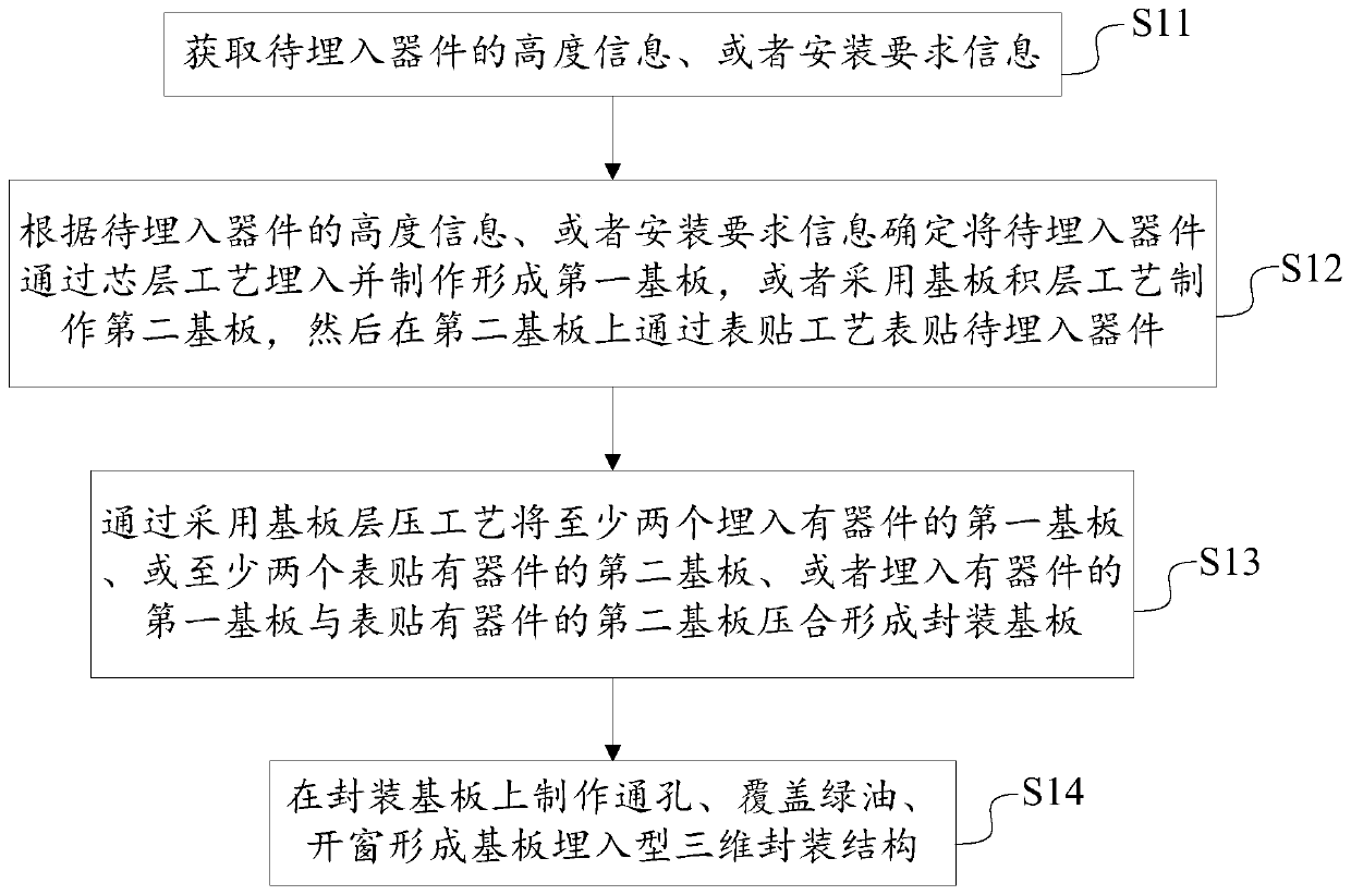
[0043] An embodiment of the present invention provides a substrate-embedded three-dimensional system-in-package method, such as figure 2 As shown, the method includes:

[0044] S11. Obtain height information of the device to be embedded, or installation requirement information;

[0045] S12. According to the height information of the devic...


PUM


Abstract

The invention provides a substrate embedding type three-dimensional system-level packaging method and structure; the method comprises the following steps that height information or installation requirement information of a to-be-embedded device is acquired; according to the height information or the installation requirement information, it is determined that the to-be-embedded device is embedded through a core layer process and is made to form a first substrate, or a second substrate is manufactured by adopting a substrate lamination process, and then the to-be-embedded device is attached to and mounted on the second substrate through a surface attaching process; at least two first substrates, or at least two second substrates or the first substrate and the second substrate are laminated to form a packaging substrate by adopting a substrate lamination process; a through hole is manufactured in the packaging substrate, and then green oil covering, and window opening are carried out to form the substrate embedding type three-dimensional packaging structure. According to the method, most of the space can be effectively saved on the surface, the packaging integration level is improved,and miniaturization is realized; and a natural electromagnetic shielding and isolation structure can be formed in the packaging structure, so that the electromagnetic interference performance of thesystem is effectively improved.

Description

technical field [0001] The invention relates to the technical field of substrates, in particular to a substrate-embedded three-dimensional system-in-package method and structure. Background technique [0002] In the traditional system-in-package technology, the assembly of the active chip can adopt the surface assembly technology of wire bonding or flip-chip welding, such as figure 1 shown. In addition, for RF chips with back gold grounding requirements, such as some RF chips with GaAs substrates, poor grounding will lead to self-excited oscillation of the chip, so flip-chip welding cannot be used for assembly, only conductive adhesive Or eutectic bonding to attach the chip surface to the corresponding position of the substrate, and then interconnect through wire bonding. [0003] During the ten years since the emergence and development of 3G mobile communication technology, the traditional system-in-package structure has effectively solved the miniaturization problem of s...

Claims


Application Information

Patent Timeline
Patent Type & Authority Applications(China)
IPC IPC(8): H01L21/56H01L23/31H01L23/48H01L23/488
CPCH01L2224/16225H01L2224/18H01L2224/32225H01L2224/48227H01L2224/73265H01L2924/181H01L2924/19105H01L2924/00012H01L2924/00
Inventor 张文雯万里兮田更新
Owner INST OF MICROELECTRONICS CHINESE ACAD OF SCI
Why Eureka
Try Eureka