

A wafer transfer and measurement system
A measurement system and wafer technology, used in semiconductor/solid-state device testing/measurement, electrical components, conveyor objects, etc., can solve problems such as excessive design and processing requirements, wafer processing defects, and many transmission parts, etc. Achieve true and accurate detection results, avoid processing failures, and ensure the effect of processing results
Active Publication Date: 2021-09-03
PIOTECH CO LTD
View PDF3 Cites 0 Cited by
- Summary
- Abstract
- Description
- Claims
- Application Information
AI Technical Summary
Problems solved by technology
During the transfer process of the wafer, the wafer will be shifted, causing the wafer entering the wafer processing chamber to not be placed in the correct processing position, resulting in wafer processing defects or even wafer scrapping
[0003] In order to ensure that the entire transfer process of the wafer from the wafer storage box into the processing chamber, the position of the wafer is accurate, the usual practice is to ensure that the offset of the wafer during the transfer process is less than the design value through structural design, the method of this method The disadvantages are: the entire transmission path is long, and there are many transmission parts involved, and the design and processing requirements for each part are too high, which obviously increases the design and manufacturing costs of the equipment; During the process, the offset value of the wafer is detected and corrected before placement to ensure the position of the wafer. This method has lower requirements for the design and processing of the transmission parts, but its obvious disadvantage is: only during transmission The position of the wafer is detected, and the deviation caused by the sliding of the wafer during placement is ignored; usually in order to improve the production efficiency of semiconductor equipment, the moving speed of the robot arm is faster, and the faster moving speed will often cause the wafer to be in the Sliding relative to the supporting part during placement; therefore, the position of the wafer after placement must be checked to ensure the processing results of the wafer
Method used
View moreImage
Smart ImageViewing Examples

Examples
Embodiment 1
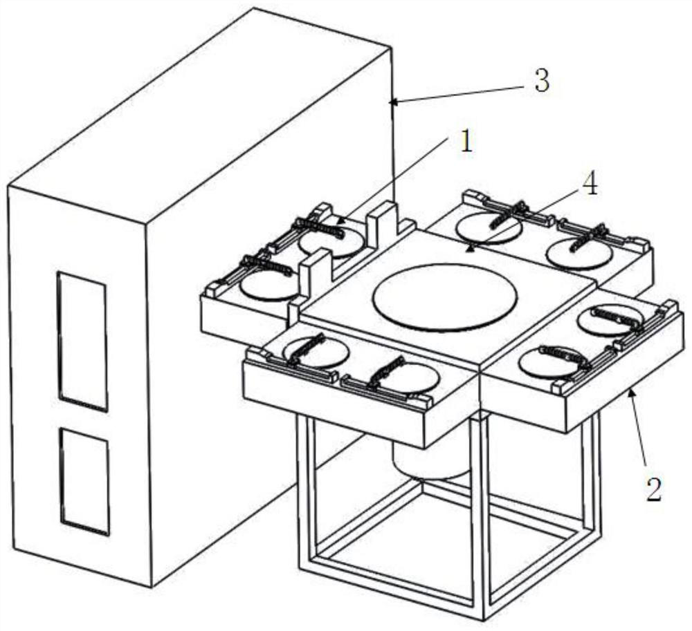
[0032] Such as figure 1 As shown, a wafer transfer and measurement system includes an atmospheric transport device 3, a wafer loading chamber 1, a vacuum transport device 4, and a wafer processing chamber 2, and the atmospheric transport device 3 and the wafer loading chamber 1 Connected, the wafer loading chamber 1 is connected to the vacuum transfer device 4, and the vacuum transfer device 4 is connected to the wafer processing chamber 2;
Login to View More PUM
 Abstract
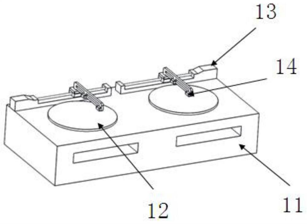
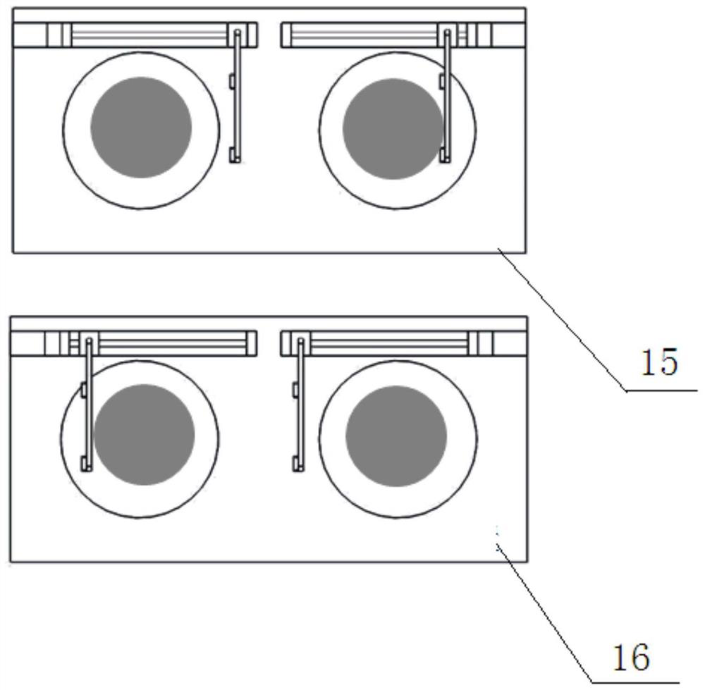
The invention relates to the technical field of transmission equipment, and relates to a wafer transfer device and a measurement method. It includes an atmospheric transport device, a wafer loading chamber, a vacuum transfer device, and a wafer processing chamber, the wafer loading chamber and the wafer processing chamber include a chamber body, a transparent window, a transmission device, and a wafer position detection equipment, the system detects when the wafer is placed in the wafer loading chamber and the wafer processing chamber; the present invention uses detection when the wafer is placed in the loading chamber and the processing chamber, and the detection result is more real and accurate, avoiding The deviation caused by the relative sliding of the wafer and the support during the placement process is eliminated.
Description
technical field [0001] The invention relates to the technical field of transmission equipment, in particular to a wafer transfer device and a transfer method. Background technique [0002] Semiconductor equipment for wafer processing usually includes atmospheric transport devices, wafer loading chambers, vacuum transfer devices, wafer processing chambers, etc. During the transfer process of the wafer, the wafer will be shifted, resulting in that the wafer entering the wafer processing chamber cannot be placed in the correct processing position, and wafer processing defects or even wafer scrapping will occur. [0003] In order to ensure that the entire transfer process of the wafer from the wafer storage box into the processing chamber, the position of the wafer is accurate, the usual practice is to ensure that the offset of the wafer during the transfer process is less than the design value through structural design, the method of this method The disadvantages are: the enti...
Claims
Login to View More Application Information
Patent Timeline
 Patent Type & AuthorityPatents(China)
IPC IPC(8): H01L21/677H01L21/67H01L21/66
Inventor王亮曹晓杰王卓
OwnerPIOTECH CO LTD