Circuit compensation device applied to fringe screen notch area

A compensating device and circuit technology, applied in circuits, electrical components, electrical solid devices, etc., can solve problems such as affecting parasitic capacitance, and achieve the effect of ensuring stability and avoiding notchmura

Active Publication Date: 2019-06-25
UNIV OF ELECTRONICS SCI & TECH OF CHINA
View PDF5 Cites 3 Cited by
  • Summary
  • Abstract
  • Description
  • Claims
  • Application Information

AI Technical Summary

Problems solved by technology

Among them, the cross-sectional view of the compensation area is as follows image 3 As shown, it includes source-drain layer (SD) 04, ILD interlayer dielectric layer 03, Gate layer (gate layer) 02, GI layer (Gate interlayer layer) 01 and poly layer (polysilicon layer) arranged in sequence from top to bottom. )00, the compensation capacitance is formed by overlapping the gate line (Gate line) and SD of each row. When the line width of the gate line (Gate line) changes, the overlapping area will change, thereby affecting the parasitic capacitance

Method used


Image

  • Circuit compensation device applied to fringe screen notch area
  • Circuit compensation device applied to fringe screen notch area
  • Circuit compensation device applied to fringe screen notch area

Examples


Embodiment

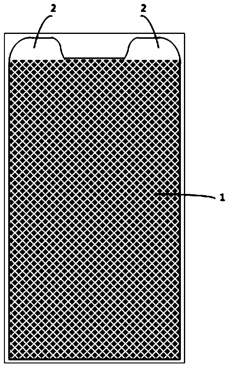
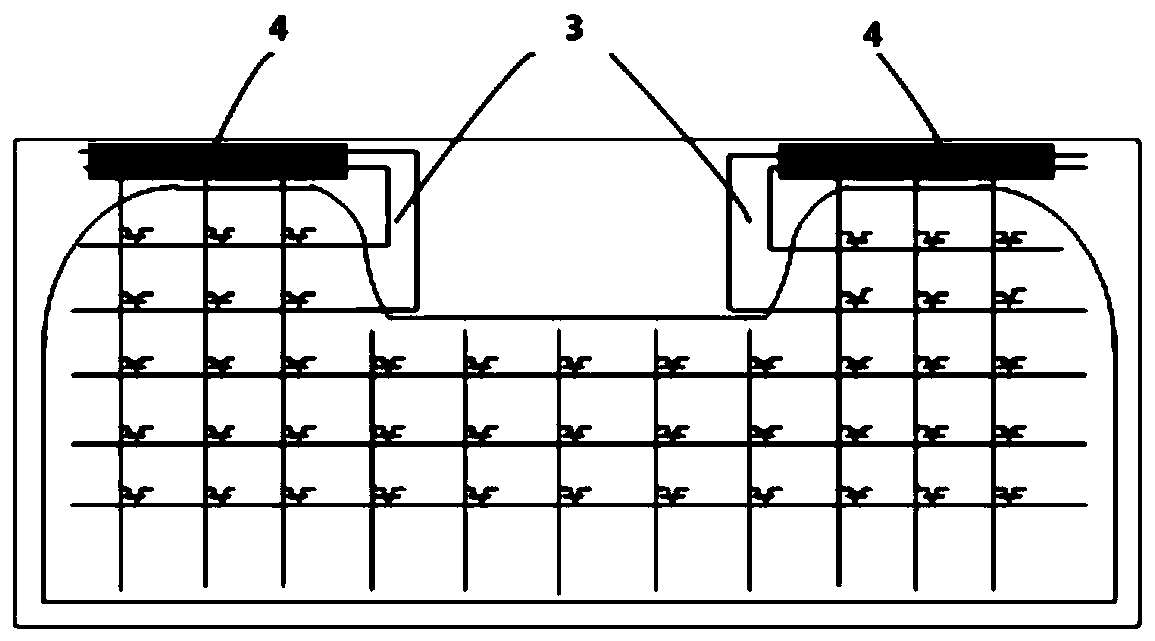
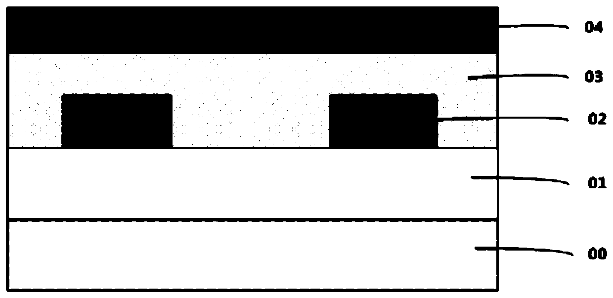
[0021] Connect the gate line (Gate line) of each row in the notch display area of ​​Liu Haiping to the outside of the AA area (active area, display area) above the panel (Panel) to form a compensation area, through Gate / ILD (Inter Layer Dielectric interlayer dielectric) / SD (Source Drain, source and drain layer, mainly used for the source and drain of the TFT of the pixels in the AA area and the surrounding SD wiring) forms a parasitic capacitance to increase the load of a single row of pixels in the notch display area. From top to bottom, the compensation device is source-drain layer (SD) 04, ILD interlayer dielectric layer 03, GI layer (Gate interlayer layer) 01 and poly layer (polysilicon layer) 00, and Gate layer (gate layer) 02 is located In the ILD interlayer dielectric layer 03. Among them, the poly layer is polysilicon with a thickness of 500 angstroms; the GI layer is silicon oxide and / or silicon nitride with a thickness of 2500 angstroms; the gate layer is molybdenum...


PUM


Abstract

A circuit compensation device applied to a fringe screen notch area belongs to the technical field of organic light emitting display. The circuit compensation device includes a source-drain layer 04,an ILD interlayer dielectric layer 03, a GI layer 01, and a polycrystalline silicon layer 00 which are disposed in this order from top to bottom. A gate layer 02 is located in the ILD interlayer dielectric layer. The gate layer is a rectangle, trapezoid, parallelogram or circle having a length-width ratio less than 2:1. The circuit compensation device, by improving an existing strip-shaped capacitor compensation into a square capacitor compensation having a length-width ratio less than 2:1, greatly reduces the influences of a process line width error on the compensation capacitor size, and thesizes of the compensation capacitors in each row can be separately adjusted so as to ensure the stability of a compensation effect.

Description

technical field [0001] The invention belongs to the technical field of organic light-emitting displays, and in particular relates to a circuit compensation device applied to the notch area of ​​an OLED "notch screen". Background technique [0002] The display screen is a device used to display images and colors. It is widely used in mobile phones and computers. With the continuous development of modern technology, the display screen is no longer satisfied with the original flat screen, curved screen and full screen. more and more attention of researchers. Among them, small and medium-sized full screens are mainly special-shaped screens, such as "notch" screens. The display area of ​​Liu Haiping includes the normal display area (such as figure 1 As shown in Part 1) and notch display area (special-shaped area, such as figure 1 shown in Part 2). From figure 1 It can be seen that compared with the normal display area, the notch display area of ​​Liu Haiping has a smaller di...

Claims


Application Information

Patent Timeline
Patent Type & Authority Applications(China)
IPC IPC(8): H01L27/32
Inventor 尚飞向勇
Owner UNIV OF ELECTRONICS SCI & TECH OF CHINA
Why Eureka
Try Eureka