Isolation structure and forming method thereof, image sensor and manufacturing method thereof

An image sensor and isolation structure technology, applied in radiation control devices, etc., can solve problems affecting the performance of image sensors, affecting the accuracy of information collection in adjacent pixel areas, affecting the quality of black level calibration of image sensors, etc., to improve performance , the effect of improving the quality

Active Publication Date: 2021-08-10
淮安西德工业设计有限公司
View PDF6 Cites 0 Cited by
  • Summary
  • Abstract
  • Description
  • Claims
  • Application Information

AI Technical Summary

Problems solved by technology

[0003] In order to ensure the accuracy of black level calibration, black level calibration pixels cannot be disturbed by external light and charges in the semiconductor substrate. Generally, metal shading is used on the photodiode in the black pixel area to prevent light from entering the black electrode. The charge in the semiconductor substrate is generated by the photoelectric charge overflow due to the saturation of the photodiode in the active pixel area. This part of the overflow charge will be transferred to the black level calibration pixel through the substrate, and then the black charge The flat calibration pixel will collect this part of the charge signal, so the information collected by the black level calibration pixel is not a real no-light reference signal, thus affecting the quality of the black level calibration of the image sensor
[0004] Similarly, an image sensor may include multiple pixel areas, and the overflow charge of a photodiode in a certain pixel area may cause interference to adjacent pixel areas, thereby affecting the accuracy of information collection in adjacent pixel areas, thereby affecting the image quality. Sensor performance

Method used


Image

  • Isolation structure and forming method thereof, image sensor and manufacturing method thereof
  • Isolation structure and forming method thereof, image sensor and manufacturing method thereof
  • Isolation structure and forming method thereof, image sensor and manufacturing method thereof

Examples


Embodiment Construction

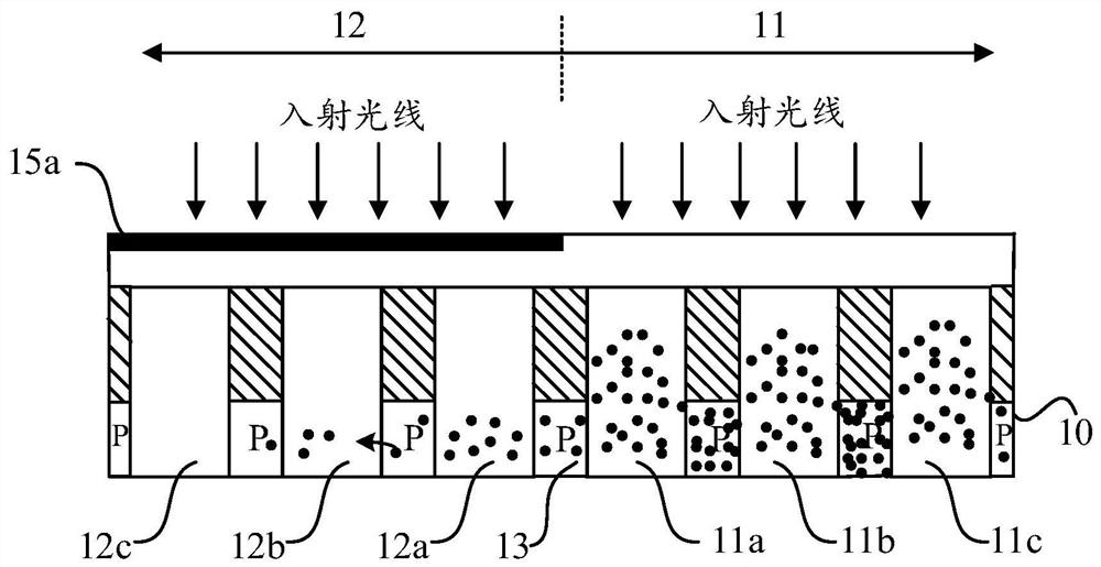
[0028] In the prior art, image sensors often include multiple pixel areas, and the overflow charge of a photodiode in a certain pixel area may cause interference to adjacent pixel areas, thereby affecting the accuracy of information collection in adjacent pixel areas, thereby It affects the performance of the image sensor, and the active pixel area and the black pixel area are taken as examples to illustrate below.

[0029] Such as figure 1 As shown, the image sensor includes an active pixel area 11 and a black pixel area 12. The pixels in the active pixel area 11 are used to perceive external light information, and the pixels in the black pixel area 12 are used as black level calibration pixels to realize the black level of the image sensor. Calibration operation. The photodiode 11a, photodiode 11b, photodiode 11c of the active pixel area 11 and the photodiode 12a, photodiode 12b, and photodiode 12c of the black pixel area 12 are separately arranged in the semiconductor subs...


PUM


Abstract

The technical solution of the present invention discloses an isolation structure for an image sensor and its forming method, an image sensor and its manufacturing method, the image sensor includes a first pixel area and a second pixel area, and the isolation structure includes: a groove The isolation structure is located between the first pixel area and the second pixel area in the semiconductor substrate; the PNP type isolation area is located between the bottom of the trench isolation structure and the bottom of the semiconductor substrate, including the first A first P-type region adjacent to the pixel region, a second P-type region adjacent to the second pixel region, and an N-type region located between the first P-type region and the second P-type region. The isolation structure can effectively eliminate the influence of the overflow charge of the photodiode in the pixel area on the adjacent pixel area.

Description

technical field [0001] The invention relates to the manufacturing field of semiconductor devices, in particular to an isolation structure and a forming method thereof, an image sensor and a manufacturing method thereof. Background technique [0002] The pixel area of ​​the image sensor may include two parts, an active pixel area and a black pixel area. The active pixel area is used to perceive and collect image information, and the information collected by the black pixel area is used as the reference information calibration in image information processing; that is to say, the real image information is equal to the information collected by the active pixel area minus The information collected in the black pixel area is also called black level calibration pixel, and this method is called black level calibration operation in the industry. [0003] In order to ensure the accuracy of black level calibration, black level calibration pixels cannot be disturbed by external light a...

Claims


Application Information

Patent Timeline
IPC IPC(8): H01L27/146
Inventor 王阳阳汤茂亮刘少东
Owner 淮安西德工业设计有限公司
Why Eureka
Try Eureka